Need ideas for high bandwidth gain stage..

GroupDIY Audio Forum

Help Support GroupDIY Audio Forum:

This site may earn a commission from merchant affiliate links, including eBay, Amazon, and others.
[quote author="Svart"]I guess I should explain what I am doing here, this circuit is gain for the output of a DDS(AD9911)(200mvP-P 50R loaded) to 2vP-P 50Rloaded into the REF port of a PLL, the AD4113. I found that during testing the difference between a 200mv(-10.5dbm) signal and a 2v(8dbm) signal is about 10dbm of phase noise at 10khz from the carrier.[/quote]
200mVpp is below the minimum ref input voltage for the ADF4113, so that's not too surprising. I have personally found those ADF parts to be more finicky than their LMX brethren, BTW.

So you don't really need any DC gain (or even point-one-dB predictable RF gain), as long as you can drive the REFIN hard enough without drooping off at higher frequencies, right? You also don't care much about linearity, IP3 and compression, as you're amplifying a (synthetic) sine wave and the first thing the signal hits inside your synth is a limiter anyway.

Solution #1: a step-up RF transformer, which could double as a balun. Something like the Mini-Circuits TC16-161T would do the job just fine.

#2: a monolithic microwave amp, like the ERA-6.

#3: a comparator, like the LT1720. Will add more jitter than #1 or #2, though.

#4: Go discrete:
pnp-difflimiter.png

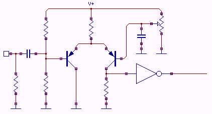
The inverter can be a single-gate LVC04. If you go an octave lower and add emitter degeneration you might even be able to use bog-standard 2N4403s; for higher frequencies I have had good luck with BFT92s in this configuration.

JDB.
 
Wow JDB, a transformer would likely do the job. I think I might have something around the lab to try. I don't have an explanation why I didn't think about using a transformer.

Brad, I could see it. I have nice agilent gear to about 5ghz.. I'll take a look and see, that is something else I didn't think about. Yes, I need to gain up the DDS output and rise/fall/settling time is important to keep phase noise down.

I don't know if I could guarantee that the offset of the PLL REF input would be exactly the same at all times regardless of termination. I'm pretty sure that it would be but I can't take that chance if you know what I mean.. A couple more cents worth of parts to ensure proper coupling is much cheaper than hardware rework on thousands of units! My idea was to offset the opamp to swing around 2.5v and IF possible I could match it to the PLL but that is not required and that would be the only case I need DC precision. You are correct about the polarity too, it doesn't matter either way, I could also invert the output of the DDS in software if needed.
 
I had a quick talk with my team partner and although we'll have to rework the output filter for the DDS, we should be able to replace the transformer we currently use for diff-single ended conversion and step up.

I think this will be the next avenue of research.
 
Regarding the transformer: isn't the C load of the ref input going to pull things down a lot? Even if you live with 200mV p-p transformed to 800mV p-p (the suggested Minicircuits one) and have a 50 ohm drive, you're looking at 800 ohms out, -3dB with 3.3pF loading.

The ADF4113, which I assume you meant, says it has 10pF max input C for the REFin's. Not sure of the typical, but that will suck things down I'd think.
 
You're absolutely right. I checked it out this morning without simulation or really thinking about it. I had a minicircuits t13-1t+ sitting around and gave that a try. Not enough..

I'm going to have to sit back and think about this one for a little while, I'm starting to get punchy and impulsive.. :roll:
 
IIRC this is one of the reasons we don't use this part anymore -- it's very picky about its REF input; it really wants to be driven by a full-swing signal, especially at higher supply voltages.

So why not use a fast comparator like the LT1720? That's what we ended up doing. 60MHz is pushing its max toggle speed (depending on supply voltage -- higher VCC leads to lower fmax), but I would recommend you to take that DDS an octave lower anyway, as that'll cut down on spurs.

JDB.
[if you do use the LT1720, keep in mind that its input common mode range doesn't go all the way up to VCC. That's the only gotcha with that part I've found in over a dozen design-ins]
 
The LNA did it! It's a little high power consumption but it works like a champ.

I got my 10db phase noise reduction and then some!

Thanks a ton everyone!
 
datasheet: 65ma
my measurement: 64ma

It's not actually that bad. I'm running it on a higher power rail and resistively dropping the voltage right now so things are a little warm. Once I can get it onto a proper rail I think things will be good to go!
 
That's not too bad.

I looked for fun at some cheaper alternative circuits using teeny discretes, but that was before I saw the hefty input C of that PLL part. By the time you push enough current through to drive 10pF well at 2V p-p and 60MHz, you probably come close to that power consumption.
 
Yeah it's not too bad, but it doubled my consumption on the 5v rail.. :green:

Now I'm up to 120ma!

:green:

I don't have anything else to put on that line so I'm good!

:thumb:
 
[quote author="bcarso"]By the time you push enough current through to drive 10pF well at 2V p-p and 60MHz, you probably come close to that power consumption.[/quote]
Only if you're trying to stay linear. Charging/discharging 10pF to a 3V3 rail at 60MHz eats 2mA (and Svart, please tell us you're not running that ADF4113 off 5V). A simple digital buffer such as the 74LVC1G04 adds 18pF of power dissipation capacitance; call it 30pF including parasitics. That's 6mA for the driver; I'd be surprised if your voltage amplification stage would eat ten times that.

A straight comparator would be faced with the same 2mA dynamic load current, plus (for the LT1720) 3.5mA static consumption plus ~2mA dynamic current, for a grand total of 7.5mA. These are 'typical' values, but they match what I've seen from samples on the bench.

JDB.
[but hey, if the LNA works for you and you can spare the current, that's fine too. Not broken, don't fix]
 
actually I am running it off of 5v for the time being. Can you elaborate on why i shouldn't? Honestly I didn't see much difference between 5v and 3.3v when testing.

Slewing a square wave that close to a sensitive circuit gives me nightmares. I had to deal with a problem with a clock line that spewed harmonics all over the place(in another RF product). I had the choice of cutting the amplitude(5v originally) or going with a sine wave oscillator. It was easier to ECO the oscillator than have people do field service.. So, in went the sinewave osc and no more harmonics.

That's why I am trying to stay sine all the way up to the PLL if I can help it. Remember, this is a hand-held device with limited space (and budget)for shielding too.

Although, JDB, I'd really like to get those current consumption numbers you posted.

I'll doublecheck my current measurements when I get in to work in the morning.
 
[quote author="Svart"]actually I am running it off of 5v for the time being. Can you elaborate on why i shouldn't? Honestly I didn't see much difference between 5v and 3.3v when testing.[/quote]
Please don't treat this as anything but badly remembered hearsay (or vice-versa), but when I was working with the part I got the distinct feeling it was originally meant for 3V3 operation only, and patched up for 5V in a very late stage of product development. One sign is the REF voltage input -- a reasonably sane 18dB acceptable input range @3V3 (0.4V-3V3), versus barely 4.5dB @5V (3V-5V). Again, this is from my vague recollection, and I may well be wrong (and it might even have been early silicon).

[quote author="Svart"]Slewing a square wave that close to a sensitive circuit gives me nightmares.[/quote]
Sure. That's another reason why I'd pick a lower DDS output range: it allows you to use slower logic, with slower edges and thus less RF energy.

JDB.
 
Thanks JDB, you have me wondering about running it on 3.3v.. My testing was simply to see how the noise/spurs changed running it on different rails. The VCO is 5v but everything else is 1.8/3.3 in the circuit so I could honestly go either way. I'll test REF input range in the morning.

Thanks again everyone!
 
It may be telling that when I try to pull up the datasheet for the 4113, it only allows me to look at a different part* :roll:

I agree that the power diss capacitance is not that scary. My thought would be that a linear stage if done correctly will have likely lower phase noise, as the CMOS in the switching stuff has typically higher low frequency excess noise.

If a bit of droop in response could be tolerated at 60MHz it might well be competitive in power dissipation, and it would almost certainly be cheaper.

However, I was pleasantly surprised when I looked at the noise of one of the Supertex DMOS parts recently, although it still didn't beat an optimized bipolar design in the high voltage compliance current source application. MOS has gotten a lot better over the years.


*Namely the ADF4154
 
JDB hit the nail on the head. When running the device on 3.3v, the REF port sensitivity becomes usable without needing to gain the DDS output. I would have read that datasheet 20 more times before I found that REF port thing. :roll:

Thanks JDB!

I tried an experiment feeding the PLL REF port with both sine and square waveforms. I saw no appreciable difference using one or the other.
 
Since this is GroupDiy I need to try swapping 1000000 different kinds of caps to find ones that have the least distortion.. :roll:


:green:
 
Back
Top