My first attempt in layout design. Any opinions?

GroupDIY Audio Forum

Help Support GroupDIY Audio Forum:

This site may earn a commission from merchant affiliate links, including eBay, Amazon, and others.

ytsestef

Well-known member
Joined
Jul 2, 2009
Messages
192
Location
Athens, Greece
I just finished my DIY UV exposure box (ex-scanner) and want to make a simple circuit to test it.
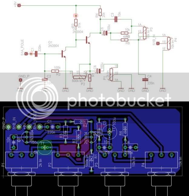
I chose to do a stompbox that is cheap, easy and useful: the Wooly Mammoth. I found the schematic and tried to make a pcb layout for it.
It is the first time I ever try to do anything like this, so I guess it will be full of errors  ::) ::) GO EASY ON ME!!  ;D ;D
I have attached a picture that shows the schematic and my pcb version. Can someone check it and point out any errors or signs of bad design or tips?

The 3-pin Molex are for connecting the pots (want them easily replaceable) and lots of input/output/switch/battery wiring is going to be off-board, so only the actual circuit is in the pcb and some holes in the upper-left corner for connections of +9V, ground, one pole of the bypass switch and one throw (the "circuit in" setting).

The components dimensions and lead spacing is based on actual products (checked with datasheet of each component)

Thanks a lot in advance for your help!! This place rocks!

EDIT: PICS REMOVED, SEE BELOW!!
 
you're referring to the right lead of R4 and the C2 to ground / Q1 emmiter to ground connections, right?
thanks a lot, i'll fix that!!

by "acid trap" do you mean that these spots may be difficult for ferric chloride removal resulting in over-etching? ???
 
Those 220nF looks BIG! Not a problem if you have a bunch of esoteric caps you want to use, but it would cost you nothing to add pads for smaller caps...

Axel
 
mad.ax said:
Those 220nF looks BIG! Not a problem if you have a bunch of esoteric caps you want to use, but it would cost you nothing to add pads for smaller caps...

Axel

Good idea!
Updated layout with eliminated acid traps and alternative 220nF capacitor dimensions. Is the whole thing ok now?? Nobody commented on whether the layout is faithful to the schematic, circuit-wise.  ???

 
I always try to make my layouts easy for home etching & building.

So I try & keep my traces at least .8mm thick, preferably 1mm. Try & keep the amount of copper to be etched to a minimum, makes etching time a lot shorter.

I always make the polarised components face the same way, all the electro caps have the pos on the left or at the top, the transistors face the same way, etc. Makes errors less likely.

I try & mount pots on the PCB to avoid flying leads, cuts construction time by a HUGE amount.

Peter
 
Make the tracks wider, and use the "miter" function to round that corners. I'm not sure about capacitor footprints but you should double check that. 100u/16v looks too big on your board. Unless you want to use 100u/63V  ;)
 
Thanks everyone for your advices and hints!!

I have attached the updated layout, using smaller footprints for everything, 1mm tracks with round corners. Q1 and Q2 are now facing in the same direction and pots are now PCB mount!!

Is it any good now???

EDIT: After posting I discovered C5- to R5 has some bad corner, consider it fixed. Also, the pot footprints have two extra pads for switch, it's there temporarily until I find some normal pot footprints, or I will erase the extra pads (and of course fix the continuity of the tracks)
 
1. Mr. Divos, who is also a member here, makes a point of not having his schematics reposted. Instead place a link to where you have the schematic from. By posting it here you also violate his copyright he has on the artwork of the schematic. Why don't you just redraw it? To work with Eagle the way it's meant to be, and I really recommend that, you will have to do that anyway.

2. It is widely considered as aesthetically more pleasing to have nothing but 45° angles in single traces. For audio it's more or less of no technical importance, but it looks better and the traces are shorter. Of course there are enough people who will have a different opinion on that.

3. Same goes for the pads, there is no need for those big oval pads. For the transistors smaller ones might even be preferred. DRC -> Shapes you can select all to be round.

4. There is still some traces you could make shorter by better component placement. You could easily put all of the components that are below the pots above them.

5. You might consider using a ground plane instead of the ground traces. Besides the shielding effect you would also save etchant (= money) and pollute the environment with less copper.


Just some food for thought. Your pcb will work without changing any of the points mentioned, but pcb design is also an art. Take pride in your work and make it look good ;).


Volker
 
Yes, pcb layouts have an ascetic quality to those of us who look at them, but IMO you time is better spent trying to please the electrons and holes. A good layout will generally look good too, but a good looking layout is not always good. 

I find it helps to visualize every trace as a resistor (especially ground traces) to get a sense for the consequences of current flow.

JR
 
volker said:
Mr. Divos, who is also a member here, makes a point of not having his schematics reposted. Instead place a link to where you have the schematic from. By posting it here you also violate his copyright he has on the artwork of the schematic. Why don't you just redraw it? To work with Eagle the way it's meant to be, and I really recommend that, you will have to do that anyway.

Volker

Thanks a lot for the time you put looking into my layout.

I'm really sorry, I didn't know any of that!!! I just found the schematic on some forum (maybe even this one), AS SHOWN. The thing is, each time I stumble upon a schematic I right-click/save it to my schematics folder. I didn't have the slightest purpose to violate someone's work or copyright. THEREFORE, ALL PREVIOUS IMAGES HAVE BEEN REMOVED!  :)
Btw, would someone help me find the original link for this schematic? I don't know where to start searching.

EDIT: OK, silly for two reasons: 1) As always google is the best place to start searching, so here is the link: http://analogguru.an.ohost.de/193/schematics/Zvex_WoollyMammoth.gif
2) The picture reads it out loud in the middle of the schematic, (C) 2007 by Gottfried Divos. I was so concentrated into getting it right, that I overlooked someone may not want this reposted. Volker is right, it IS owned by Gottfried Divos. Now I know... Sorry!  :-[

This thing aside, thanks a lot for your tips, I will try to take them into account and come up tomorrow with something both good and aesthetically good.
As for redrawing the schematic with eagle and associating it with the board, the basic reason for not doing this (yet) is that I am only a guy with some skills at soldering and  producing/mixing/music generally. I am a total newbie when it comes to electronics, but I have become so obsessed with it already, that I want to improve, thus the countless newbie questions (though I am already into reading electronics books). I am even more of a newbie in using Eagle, and I didn't know many things mentioned in this thread, including changing pads, track width, using ground planes, so this has been really helpful! Thanks a lot everyone!
 
OK, what about this one?
I changed the layout and now all components except one resistor are above the pots. I also did the 45 degree angle thing, changed all pads to round ones (no oval pads anymore) and added a ground plane. I don't know if the method I used is the right one or just a pseudo-ground-plane, though.
 

Attachments

  • board.jpg
    board.jpg
    226.5 KB · Views: 71
It is also nice to have all  the connections along one edge of the board, means longer traces but I much prefer the neatness of it.

heads up: the left hand 10nF has only 1 pin connected......

Peter
 
the left hand 10nF has only 1 pin connected......
Before you start designing BRD file check your sch file with ERC function. It will show you all logical errors. That's the way to avoid such a mistakes.
 
Looks way better! Best way to make a ground plane in Eagle: first remove all your ground traces ('RIPUP gnd'), then draw a polygon around the board, name it GND, do ratsnest (that calculates all polygons and all connections left to do). Choose appropriate isolate settings in the properties of the polygon. Use thermals and don't use orphans. To put the polygon back in non-rendered state, just do RIPUP on one of the edges.

As for what Peter stated: mistakes like that won't happen if you work with a proper schematic. It's really not too complicated, there is an easy step by step tutorial in the Eagle manual you can download on their site. And for more complex projects this is really mandatory. To count on checking every connection by hand would drive me totally nuts. And as you will see, the routing process is much more comfortable and will take a little fraction of the time spent before.


Volker
 
Right!

I did it the proper way now (I hope). I am posting both the schematic and the board that came out of it.
The only problem I had was the with the ground plane. I did it exactly as volker said, the plane was filled but it did not touch any of the ground contacts. ??? I did it again without using RIPUP on the gnd tracks and that's what I got!

I am not sure if I did it correctly (even in the schematic) and I am to tired to see any problem. That, or I finally got it right!  ::)

I also saw some pics of stompbox guts on the web and most of them seem to be using pots arranged as shows in my layout. I decided to go that way, I'm afraid the 9V battery, the jacks and the switch won't fit if I did it with vertical pots as shown in my previous post.
 

Attachments

  • board.jpg
    board.jpg
    270.1 KB · Views: 45
It takes a while to get it right and then you will just improve. Just keep at it. When I look at your first and then last version its an amazing progress! (I wish I was as fast a learner).

In the meantime here is a link that has practical knowledge to impart. Good for beginners and those that forget some fundamentals.

http://tangentsoft.net/elec/movies/

Jim
 
Bluzzi said:
It takes a while to get it right and then you will just improve. Just keep at it. When I look at your first and then last version its an amazing progress! (I wish I was as fast a learner).

In the meantime here is a link that has practical knowledge to impart. Good for beginners and those that forget some fundamentals.

http://tangentsoft.net/elec/movies/

Jim

Thanks for the comments! The link is awesome too, very useful.
I just want to know, is the last one at least usable? Will it work?? I know in some time from now I'll be making much better boards, but I wonder if I should etch this one...
 
I just want to know, is the last one at least usable? Will it work??
Well you can improve a bit your design by moving few components . For example, you can make more space between P1 and P2 to make it lower position C6 (green) or use smaller footprint (i still believe that 100u/16v is smaller nowadays).  Than you will make possible groundplane to spread between tracks . Same with  Planes U made (marked with red ) are not grounded and they are acting like antennas. ;) Use "isolate" function for groundplane polygon to make it possible to spread. Also, with polygon track width you can do something about.
On schemo you don't need dots marked with red. U need that dots only when 3 or more points have to be connected. It will not make any problem but looks ugly  ;)

BTW, I didn't compare your schemo with original but I presume that they are identical.  ;D

board.jpg
 

Latest posts

Back
Top