Solo-in-place schem?

GroupDIY Audio Forum

Help Support GroupDIY Audio Forum:

This site may earn a commission from merchant affiliate links, including eBay, Amazon, and others.
The circuit was part of the input module, and my recollection is that it drove the channel fader directly, there was no significant amount of intervening cable. By itself, the uA739 doesn't have a particularly ballsy output, so the buffer just serves to raise its current capability. API also had the habit of a certain amount of overkill, and I'd just call this circuit evidence.

I think that history vindicates them for the overkill.

Remember that although my circuit doesn't blatantly show it, the original used a uA739 dual opamp, which is externally compensated, and there was a place for input compensation as well as around the output stage. The compensation components are noted in the "Notes" part of the schematic. I used TL082s in the drawing because the schematic symbol was available and because I was far too lazy to create a new symbol for the 739. TL082s weren't even a glimmer in someone's eye in 1972.

tv said:
It's obvious that C11 is "compensating" for something, but for what exactly? The fact that the C9 isn't directly in UA1s FB path (ie connected to pin1 instead of the output Q's emitters) seems odd as well - if output is shorted or driving some cable's capacitance this would seem odd regarding that the whole circuit otherwise seems of "baroquesque" proportions. Designers surely have accounted for thet scenario. But, "they" surely know why it is as it is.
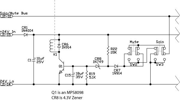
 
Thats what I originally thought:

Namelly, if the output gets short-circuited, or capacitively loaded, what we get out of the diamond buffer is -very- similar to two baxandall's super-pairs on top of each other, but now Q2 and Q4 acting in common-emitter config - not anymore "mere" common collector followers.. if you visualize this scenario (their emitters get "grounded" at AF/HF thru C3). The C11 then -locally- applies NFB at high frequencies -within- the diamond buff., which in this scenario acts as a twin super-pairs, which are said to be prone to self-oscillation..

http://www.groupdiy.com/index.php?topic=38094.msg476203#msg476203
 
rickc said:
I realize that often there is a difference between what appears on a shematic, and what happened in production, so I was just going to see if the capacitor was present on the board that I reverse engineered.

Since the capacitor  runs from the collector of the output device, and thinking of the collector resistor as a partial collector load (so there is *some* signal developed there), that would amount to negative feedback to the input of the output buffer. So maybe it is a bit of compensation to make the whole thing stable once it is wrapped in the overall feedback loop of the opamp?

=========================================================================

tv said:
Thats what I originally thought:

Namelly, if the output gets short-circuited, or capacitively loaded, what we get out of the diamond buffer is -very- similar to two baxandall's super-pairs on top of each other, but now Q2 and Q4 acting in common-emitter config - not anymore "mere" common collector followers.. if you visualize this scenario (their emitters get "grounded" at AF/HF thru C3). The C11 then -locally- applies NFB at high frequencies -within- the diamond buff., which in this scenario acts as a twin super-pairs, which are said to be prone to self-oscillation..

http://www.groupdiy.com/index.php?topic=38094.msg476203#msg476203

I'm not sure what schematic you guys are talking about.

The transistor buffer in the soft switch circuit posted by Rick C, is a fairly straight forward compound darlington connection. Using one polarity device for the first transistor and opposite polarity for the second transistor, gives a nice correction for the 4x Vbe drops, so the two +Vbe cancel with the two -Vbe and we end up with a nominal 0V input to output, with class AB bias set by the emitter resistors on the first pair. The 200 ohm resistors in the collector legs of the output pair, act as crude current limiting to protect against short circuits.

This Darlington emitter follower has no voltage gain (technically less than 1x) so there is no voltage gain in the buffer to roll off.

Ignoring the load on that output driver, the 47pf C from the output of the opamp is connected to +15 with 200 ohms in series.  When we put a resistive load or capacitive load on the driver, the voltage at the 200 ohm resistor changes. For a 600 ohm resistive load (possible if that output node sees outside world), that 200 ohm resistor will swing .33x of the output in the opposite direction. This will effectively make the cap look 33% larger,, not a big deal. For a capacitive load it can be more significant, at 47pf load, we have 2x the effective capacitance reflected back to the opamp output.

I regret killing this many brain cells over this. It isn't going anywhere promising. Another 5 minutes I won't get back, I googled up a data sheet for the old ua739 and it only had a single PNP output stage operating class A, coincidentally with a 200 ohm emitter resistor. The 739 had 3 compensation pins, two across an internal LTP, and one pin on the base of the output device to add some lag there. This RC may be some remnant output stage lag compensation for the former ua739 that serves no function with modern opamps..

I remain unconvinced this cap (as drawn) is doing anything useful in this circuit, and perhaps some harm.

JR
 
Come on... you coudn't kill -that- many cells over this one.

However, to make it easy for all to follow my (seemingly lethal for brain-cells) flow of thoughts, I drew a little diagram to illustrate what I see that could happen in case the output gets shorted (or there is a capacitive load).

This is one half of the "diamond", as I said, and from whatever angle you look at it, in this config it looks suspiciously similar to baxandall super-pair, as I said.

I (cough) apologize for all the headache that I caused.. 8)
 

Attachments

  • one_half_diamond.png
    one_half_diamond.png
    1.5 KB · Views: 24
tv said:
Come on... you coudn't kill -that- many cells over this one.

However, to make it easy for all to follow my (seemingly lethal for brain-cells) flow of thoughts, I drew a little diagram to illustrate what I see that could happen in case the output gets shorted (or there is a capacitive load).

This is one half of the "diamond", as I said, and from whatever angle you look at it, in this config it looks suspiciously similar to baxandall super-pair, as I said.

I (cough) apologize for all the headache that I caused.. 8)

OK, that proves we're looking  at the same schematic.  The buffer is a dual polarity Darlington emitter follower. If anything similar to a class AB amplifier output stage, but with simpler biasing. 

The voltage gain from input (base) to emitter output is <1, so there is not excess voltage gain to scrub off for stability.

The cap from base to ground, or base to collector, if anything will add phase shift and lag to the node.

In practice capacitance at that point, inside an overall NFB loop will make the amplifier less stable not more.

This may be some remnant of old 739 compensation, but that cap if anything is making the buffer, less of a buffer, and the circuit as drawn probably less stable.

It appears we need to agree to disagree since we are looking at the same schematic and drawing different conclusions.


JR

PS: a half of a something else, is not a something else.
 
I looked thru my API folder last night, and this same buffer circuit was used in several other places through their products. It's also found inside the 550A equalizer; used as a buffer between the equalizer blocks. In that application it isn't wrapped directly around an opamp.

The 47p capacitor is present in each case.


JohnRoberts said:
tv said:
Come on... you coudn't kill -that- many cells over this one.

However, to make it easy for all to follow my (seemingly lethal for brain-cells) flow of thoughts, I drew a little diagram to illustrate what I see that could happen in case the output gets shorted (or there is a capacitive load).

This is one half of the "diamond", as I said, and from whatever angle you look at it, in this config it looks suspiciously similar to baxandall super-pair, as I said.

I (cough) apologize for all the headache that I caused.. 8)

OK, that proves we're looking  at the same schematic.  The buffer is a dual polarity Darlington emitter follower. If anything similar to a class AB amplifier output stage, but with simpler biasing. 

The voltage gain from input (base) to emitter output is <1, so there is not excess voltage gain to scrub off for stability.

The cap from base to ground, or base to collector, if anything will add phase shift and lag to the node.

In practice capacitance at that point, inside an overall NFB loop will make the amplifier less stable not more.

This may be some remnant of old 739 compensation, but that cap if anything is making the buffer, less of a buffer, and the circuit as drawn probably less stable.

It appears we need to agree to disagree since we are looking at the same schematic and drawing different conclusions.


JR

PS: a half of a something else, is not a something else.
 
I know it has been a while, but I wanted to post the scheme I finally ended up with. It has been working great for the last few months. I included two caps in red that I don't actually have installed. I was wondering what anyone thought about adding them; it's really pretty quiet, but if I turn everything up, I can here the pop. If anyone thought that adding either of these caps would help with that, I would give it a try. Thanks and Best, Ben
RelaySolo-In-Placepluscaps.jpg
 
jsteiger said:
Hey Ben,

I have been using the following control circuit that I discovered in my console. Kinda like John mentioned!  ;)  Anyhow, it is for mute and destructive solo. Some minor rework would easily provide a dedicated stereo solo bus for non-destructive SIP. The parts are cheap and plentiful. Works like a dream. I like the TQ2's. Q1 is an NPN.

relay-control-circuit.jpg


Oh, and out of respect for JR, I always try to spell bus correctly.  8)

Cheers, Jeff

Hi this is my first post on the forum. Im hoping to build a 32 in/out solo mute box in a 1u case.
I/O on Dsubs.

mainly for tracking and having solo and mutes right to hand next to my pre's.

I pilfered jeff's schem (hope you don't mind jeff :) ) and wondered...

the 1n4004 and 10uf cap just at the start of the chain.
are there any noise or durability issues with having the relays active most of the time?
and will adding these leds make a difference.


Thanks in advance,

Rick

PS Hope im not hijacking this thread.
 

Latest posts

Back
Top