Silkscreen PCB experiment

GroupDIY Audio Forum

Help Support GroupDIY Audio Forum:

This site may earn a commission from merchant affiliate links, including eBay, Amazon, and others.

livingnote

Well-known member
Joined
Aug 12, 2007
Messages
1,048
Location
Berlin, Berlin
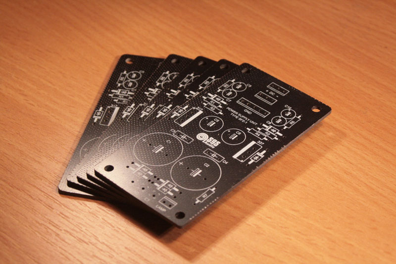
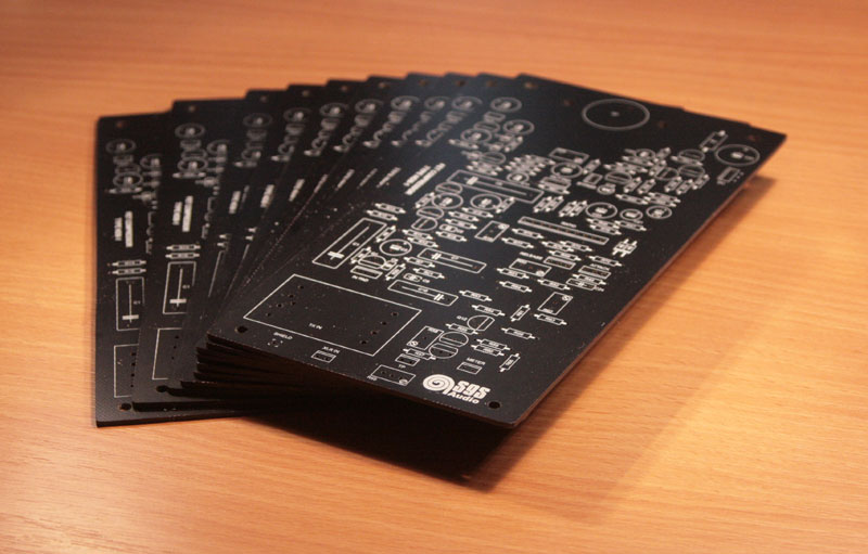
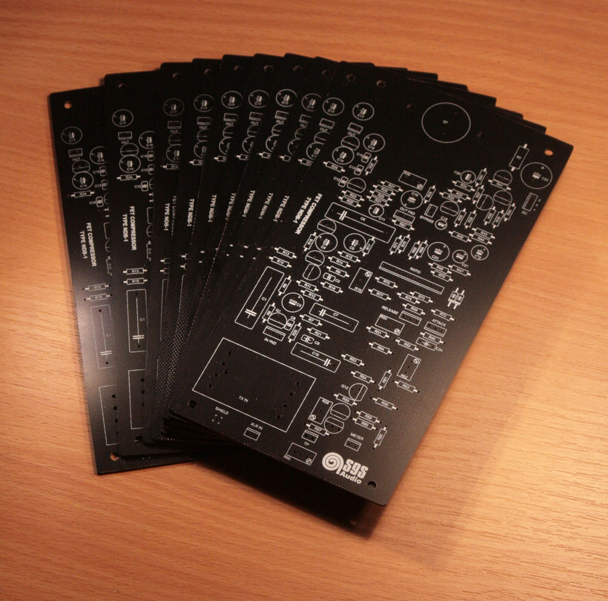
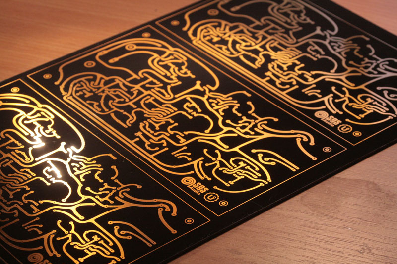
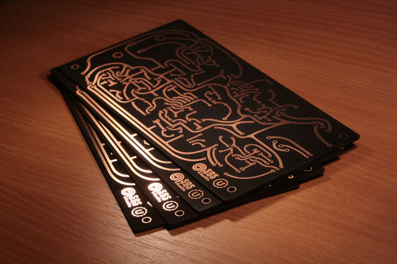
Henrik from Kalkyl at SGS ordered a somewhat bigger run on PCBs a few weeks ago and wanted to have silkscreen,
so considering that the run was big enough to go out and experiment, I went to town on it - the output was a
pdf and after having a great time playing with the traces, I set out to find a silkscreen guy who could do it...well
long story short, 100 things happened that weren't expected and things just kept getting delayed more and more,
but Henrik was totally cool about it all, so I was able to really take my time getting the details worked out:
sgs1.jpg


sgs4.jpg


sgs2.jpg


sgs3.jpg


sgs5.jpg


It was the biggest run I did so far, and I'm really happy with how it turned out. Great to see how much territory
you can cover just with the work of your own two hands if you put your mind to it. I ended up nixing anything
you could call "profit" doing it, but it was fine for me because I learned so much new stuff in the process.

Cheers to Henrik for such a cool project, and looking forward to what comes next :)
 
Oh-lala! ROUNDED corners!

Now, I'm your True Fan.
http://www.kk.org/thetechnium/archives/2008/03/1000_true_fans.php
 
I see huge amounts of spiritual and intellectual profit there.
Are those boards like, 3 mm thick?
Wonderful!
Mike
PS: let some hair grow back before you embark on screening the solder mask. . .
 
beautiful work as per usual Lukas,

you are a true artist and craftsman!
 
Wow, that just makes me feel great :) But whoa while I was on it there were so many things where
"oh god no now THIS" I started seriously thinking "how smart was it" but lord I wanted silkscreen
myself.

Really interesting article by Kelly, I remember thinking once too, "you know, screw the big time.
For me the big time is having all these cool electronics guys around"...the whole thing is still on
kinda thin ice but with the starting-to-get-proper system of organization at least it's really a reliable
and professional service like you'd expect from major webpages.

My favorite of them all is when people use my service to work together. I keep seeing it in the way
you'll have these design guys working on something, and then going "hey Lukas can you do this and
then send it there, there and there?"

One thing I've learned is that there's this magic that happens when the right guys get together,
hanging on the phone for ever talking about some concept and then working together to make it all
happen. When it suddenly does then it's like an epiphany, and because it's synergistic nobody can
really quite explain where that came from now, or take credit the way they're given, all anybody
knows is that every dolt can hear it from across the street. It's this musical-instrument-building
component that's so amazing and difficult to repeat, but awesome if you totally nail it.

So basically my idea is to just generally remove as many obstacles as possible from doing that.

@kooma - not sure, but iirc it was something of theirs.
 
Hey Lukas.
This is great man!
I was thinking while working....Man I wish Lukas would do Silkscreening soon...
The same day you show up this ....incredible...

Be prepared man!
 
Cool!

Yeah - soldermask I'm still on the picket fence about because in a way I really
don't see how it helps DIY - I mean, pretty much my whole desk was made without
it, and it's great to be able to get at everything, and make traces ultra-fat and durable
with solder, rather than some 35-70µ copper and then a thin layer of HAL with "access
denied-varnish" on top, but then again that's just me.

Silkscreen is so important it just can't be left out over the long haul, considering you
wanna always be able to repair it, and for me that means stamping both the component
names and the values on it so you're always in broad daylight about what's going on.

Thing is - outsourced like this is pretty heavily expensive (consider it cost me 180€ for
this run) and a lot of that money is setup charge...for the moment that means it's still
kinda "up there" but what would totally rock would be if I could do it myself. You basically
only need one color and the process is very similar to etching with all the photo-litho
stuff going on, so...who all here has experience in this area? I might go to a workshop
here in Berlin to learn how to do it the right way, iirc mom was at one about a year ago...

But all in all it's a very humbling and awesome experience to see all this brainpower
you guys put in your designs, makes it a real treat and honor to have the position of
"forum etcher" for sure.

@sodderboy - it's actually only 1.5mm FR4, but really serious stuff. I'm thinking of
including both the base material and the drill bits I use into my shop, when peeps need
to drill something out then it's good to have the right bits to use - I even discovered
how different tungsten carbide can be, and these just dive right in. And of course etching
with this stuff is complete and utter fun. Might make a youtube video one of these
days when the homepage is up and running, like "how to build a kickass lab and
etch like the big time" :)
 
Yup, SMD for sure. I wasn't thinking in that direction at all...but
I do guess it'll be a while before I can do that...both soldermask and
silkscreen do eat up set up time pretty hard...
 
livingnote said:
Yeah - soldermask I'm still on the picket fence about because in a way I really don't see how it helps DIY

In addition to it being necessary with SMD (to prevent shorts between adjacent pads), the soldermask also helps keep the exposed copper from corroding.

-a
 
Wow that is so amazing. I was always just going with what I love to do, thanks for all the
appreciation. I was always kinda not sure how it would be recieved but makes me feel great
to be here.

Yeah the Epson is pretty darn cool. Maybe there's also a photochemical way of silkscreening,
like, the same principle as soldermask, something you can laminate on, expose, develop, harden.

>>the soldermask also helps keep the exposed copper from corroding.

Well see that's the funny thing - you can't stop most copper from corroding whether
there's laminate on it or not. My supplier once made a real point out of using the right copper
because it all shines just the same - but on the stuff I work with, the copper forms a
ca. 3µ oxide layer which self protects, while many material suppliers use whatever fit the
budget, and that corrodes too but from the inside, which soldermask just makes worse.

I was pretty surprised to find that out myself because here I was all "yeah great let's go
and have PCBs fabbed off my stuff", but the more I learned about it the more I went "yeah
but personally I'd still etch and retrace the ones I use for myself". So here was the clinch,
"right, for yourself you'd build it that way, but all them you'd sell something different".

Knowing that P2P rocks the way it does, I don't get why PCBs for serious studio DIY should
be 35-105µ with ultra-thin HAL when it can have nice thick soldered traces you can access
anytime? I mean, Lorlin or Elma, 20€ difference, that I can understand, but redrawing
a PCB trace with solder costs next to nothing and performs like nothing else.
Obviously if you have a power line running below a SOP then you don't want to reflow the
bugger together, or for fab assembly in general. But here in DIY we can do stuff that's so
amazing with PCBs, soldermask would be all backwards.

Still though that's just my personal philosophy on building, maybe for soldermask something
dark blue semi-transparent?
 
Back
Top