chunger
Well-known member
Hello,
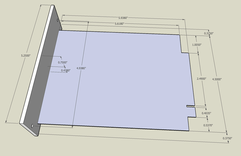
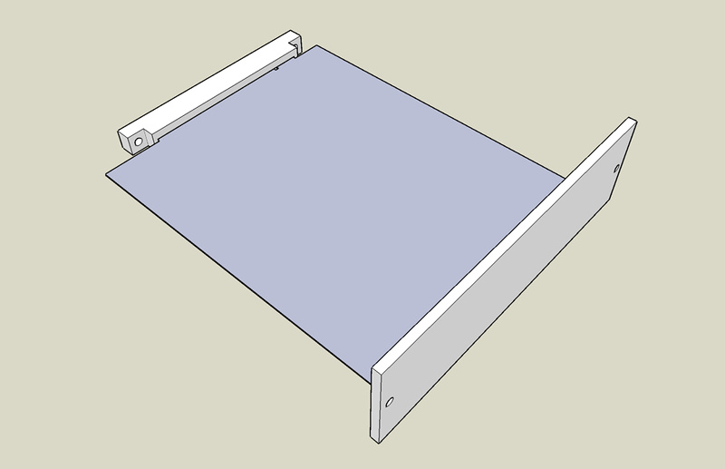
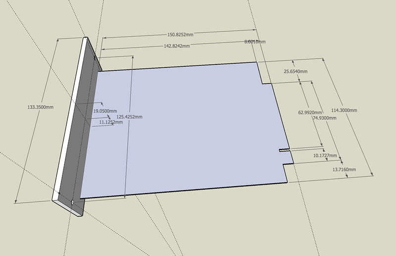
I'm working on getting some small (1 and 2 slot) 51X standard cases fabricated, and wanted to make sure that my underlying assumptions about the card/slot dimensions are correct. Please excuse the PCB that has no thickness at this point. I'm just trying to make a template to start from.
I obtained a lot of my dimensions from a file posted in the gdiy gmail account and am guessing at a few others based on measurements from one of Jeff Steiger's vp312 and vp26 boards.
I want to make sure I'm starting from the most accurate measurements possible before proceeding.
Oh, btw. . . yes, I'm biting off more than I can chew, but nobody has a product or kit that fits my application, so nothing ventured, nothing gained.
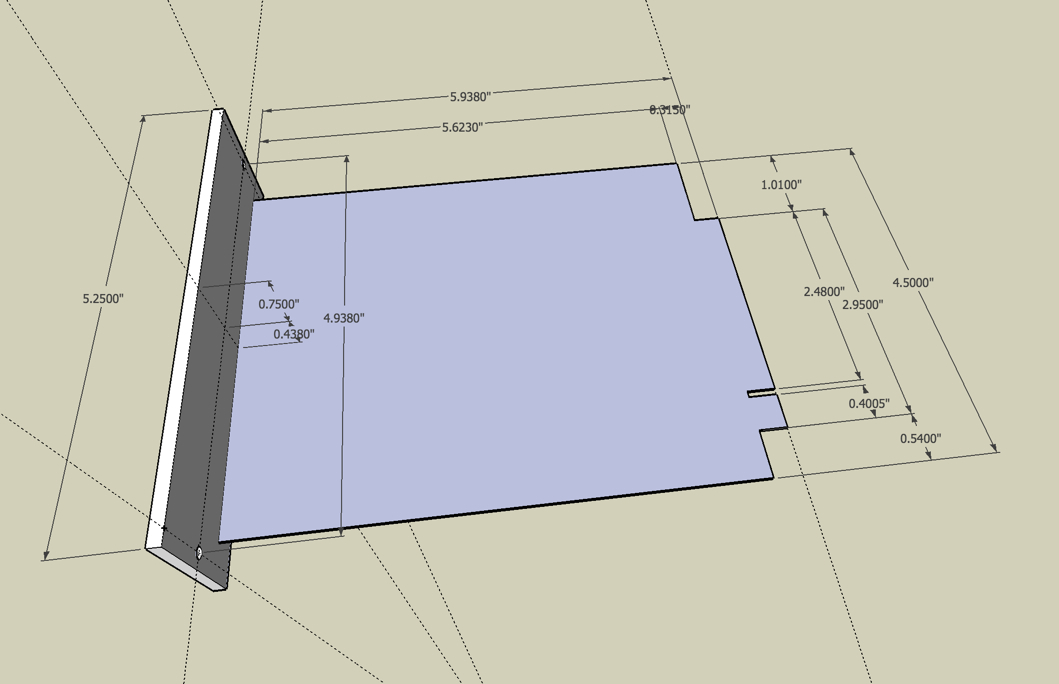
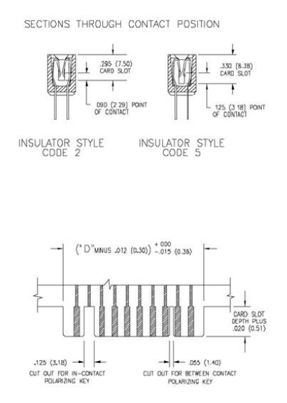
I assumed the original API 500 standard has the card slot centered on the card and the 51X goes from 15 to 18 positions adding those on the bottom side of the card. Moving forward, next I should precisely locate my PCB edge connector and I'll have all my critical mount points set and can determine case dimensions and PCB location relative to those set parameters.
I'm working on getting some small (1 and 2 slot) 51X standard cases fabricated, and wanted to make sure that my underlying assumptions about the card/slot dimensions are correct. Please excuse the PCB that has no thickness at this point. I'm just trying to make a template to start from.
I obtained a lot of my dimensions from a file posted in the gdiy gmail account and am guessing at a few others based on measurements from one of Jeff Steiger's vp312 and vp26 boards.
I want to make sure I'm starting from the most accurate measurements possible before proceeding.
Oh, btw. . . yes, I'm biting off more than I can chew, but nobody has a product or kit that fits my application, so nothing ventured, nothing gained.

I assumed the original API 500 standard has the card slot centered on the card and the 51X goes from 15 to 18 positions adding those on the bottom side of the card. Moving forward, next I should precisely locate my PCB edge connector and I'll have all my critical mount points set and can determine case dimensions and PCB location relative to those set parameters.




![Electronics Soldering Iron Kit, [Upgraded] Soldering Iron 110V 90W LCD Digital Portable Soldering Kit 180-480℃(356-896℉), Welding Tool with ON/OFF Switch, Auto-sleep, Thermostatic Design](https://m.media-amazon.com/images/I/41gRDnlyfJS._SL500_.jpg)


