First ever PCB layout

GroupDIY Audio Forum

Help Support GroupDIY Audio Forum:

This site may earn a commission from merchant affiliate links, including eBay, Amazon, and others.

ramshackles

Well-known member
Joined
Dec 18, 2011
Messages
521
Location
Riorges, France
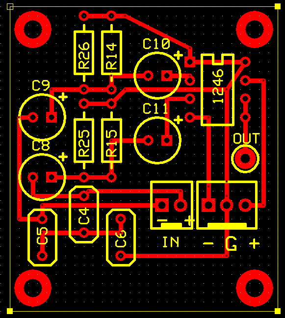
I tried having a go at pcb layouts for the first time today, with the idea that at some point I might be able to etch my own stuff or whatever.

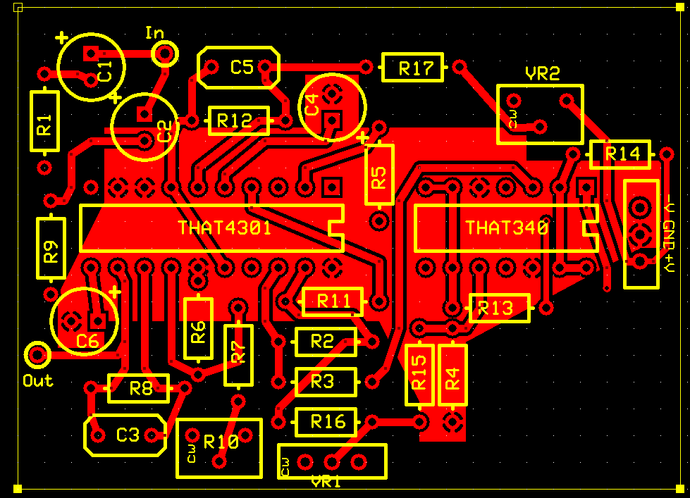
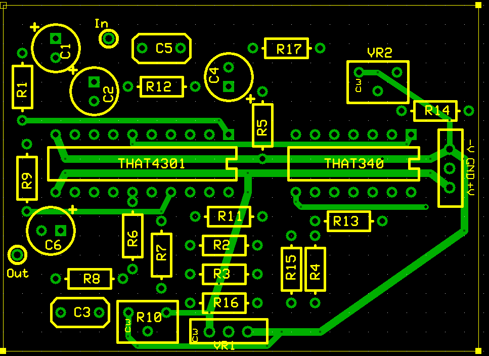
I wanted to start fairly simple, but still useful, so I had a go at the 'One Knob Squeezer' from THATcorp:
http://www.thatcorp.com/datashts/dn125.pdf

I pretty certain I've made some glaring mistakes. Opamps are certainly very tricky to deal with as how they look/are 'wired' on a schematic is very different to how they actually are!
I'm sure that my layout is not nearly as neat/well structured/'beautiful' as it should be - any tips on that?

There are certain times when you really need a teacher to check your work...are there any professional pcb checking services/people out there??

Here are the pics (it seems you can export the layouts from easypcb so these are screen dumps):

TopLayer_zpscdeae081.png


bottomlayer_zps5cc9dc8c.png
 
Couple of notes (I design schematics and then do my own PCB's as part of my job)

Your ground plane is severed in a couple of places, which is a big problem.  The only place where ground is connected externally that I can see is to the far right of the board where you have V+ Gnd V-.  However your V+ trace then slices through the ground plane meaning it has no way of getting to the rest of the pins on the board, it's on an island and none of the other components can get to it.  To the left of that you have just floating plane that isn't connected to anything at all since it's separated by traces.  Looking further you can see places like C6's - pin which are connected by just a slim little bit of plane to the rest of the plane, which will act like a resistor and create a big issue.  This occurs several other places throughout your layout.

One solution would be to get rid of it entirely and run traces, since it doesn't look like you have any fast edge rates that would require the plane in the first place.  Another solution would be to cover both top and bottom layers entirely with ground plane and then stitch them together with ground vias around the edges and throughout the board in a grid pattern, however that is more of a solution for RF designs where you have fast edge rates that need DC planes.

Either way you need to redo the grounding.

Finally I would recommend moving C4 as close to Pin 5 of the 4301 as possible, similar to how you have C6.  Bypass caps need to be as close to the pin they are bypassing as possible to be effective.

Once you get your ground fixed I'll take another look, good luck!
 
millzners said:
Couple of notes (I design schematics and then do my own PCB's as part of my job)

Your ground plane is severed in a couple of places, which is a big problem.  The only place where ground is connected externally that I can see is to the far right of the board where you have V+ Gnd V-.  However your V+ trace then slices through the ground plane meaning it has no way of getting to the rest of the pins on the board, it's on an island and none of the other components can get to it.  To the left of that you have just floating plane that isn't connected to anything at all since it's separated by traces.  Looking further you can see places like C6's - pin which are connected by just a slim little bit of plane to the rest of the plane, which will act like a resistor and create a big issue.  This occurs several other places throughout your layout.

One solution would be to get rid of it entirely and run traces, since it doesn't look like you have any fast edge rates that would require the plane in the first place.  Another solution would be to cover both top and bottom layers entirely with ground plane and then stitch them together with ground vias around the edges and throughout the board in a grid pattern, however that is more of a solution for RF designs where you have fast edge rates that need DC planes.

Either way you need to redo the grounding.

Finally I would recommend moving C4 as close to Pin 5 of the 4301 as possible, similar to how you have C6.  Bypass caps need to be as close to the pin they are bypassing as possible to be effective.

Once you get your ground fixed I'll take another look, good luck!


Thanks
I intially had the ground plane covering the whole pcb, but then reduced it, obviously missing that this caused it to be cut! Thanks for pointing it out.
Would just filling the whole pcb again with a ground plane be a solution? Seems like in order to lay traces I would need to rethink the whole thing
 
You need to connect the gnd pin to all the ground points in your board, make sure all this is happening... current should have a path from each point in the board to your connection to the rest of the world.

JS
 
ramshackles said:
millzners said:
Couple of notes (I design schematics and then do my own PCB's as part of my job)

Your ground plane is severed in a couple of places, which is a big problem.  The only place where ground is connected externally that I can see is to the far right of the board where you have V+ Gnd V-.  However your V+ trace then slices through the ground plane meaning it has no way of getting to the rest of the pins on the board, it's on an island and none of the other components can get to it.  To the left of that you have just floating plane that isn't connected to anything at all since it's separated by traces.  Looking further you can see places like C6's - pin which are connected by just a slim little bit of plane to the rest of the plane, which will act like a resistor and create a big issue.  This occurs several other places throughout your layout.

One solution would be to get rid of it entirely and run traces, since it doesn't look like you have any fast edge rates that would require the plane in the first place.  Another solution would be to cover both top and bottom layers entirely with ground plane and then stitch them together with ground vias around the edges and throughout the board in a grid pattern, however that is more of a solution for RF designs where you have fast edge rates that need DC planes.

Either way you need to redo the grounding.

Finally I would recommend moving C4 as close to Pin 5 of the 4301 as possible, similar to how you have C6.  Bypass caps need to be as close to the pin they are bypassing as possible to be effective.

Once you get your ground fixed I'll take another look, good luck!


Thanks
I intially had the ground plane covering the whole pcb, but then reduced it, obviously missing that this caused it to be cut! Thanks for pointing it out.
Would just filling the whole pcb again with a ground plane be a solution? Seems like in order to lay traces I would need to rethink the whole thing

Pouring ground in this design seems to just be the convenient thing to do, but not the best thing to do. At some point you have to consider the path each ground pin has to the external ground connection, and it's not always a straight shot.  If you can stomach a redesign that includes a ground bus from left to right you'll have a better ground scheme and more confidence you know where the return currents are.

Ground fill does more than just get ground to each pin, it changes the impedance of the traces it surrounds and it allows cross talk from noisy sources to sensitive signal traces that would otherwise be far enough apart to not have this issue.  In RF designs you'll see ground fill because you absolutely need it for a variety of signal integrity reasons and you then work around the problems it creates.  In this design you don't gain anything except convenience but you still have all the drawbacks.

My recommendation is a big fat ground bus trace (~60 mils thick) connecting everything with smaller traces so you give each ground pin one single solid connection to the external ground.  I would also turn off 45 degree traces and make everything perpendicular/90 degree angles; it makes routing easier to visualize and easier to look at once you're done.
 
Thanks a lot for the comments, they are helpful.
I decided that as it's my first experience with pcb layouts, I should start EVEN simpler. I still wanted to do something that could be practical/useful for me to use though, so I decided to try the line input section of another THAT schematic:
http://www.thatcorp.com/datashts/dn140.pdf

Page 12, fig 7.
Just the line input, so no switch and no mic in.

I included all 4 of those 100K resistors in the layout, but am I right in thinking that two 50K resistors could be used instead?

So, the ground on this is connected by traces, not a plane (much easier to do on this one) and I've tried to use right angles where I can:

1246LineIn_zps3950215b.png


And I will come back to the 'One Knob' when I'm getting good at these simple layouts...
 
Back
Top