Stupid Mistake

GroupDIY Audio Forum

Help Support GroupDIY Audio Forum:

This site may earn a commission from merchant affiliate links, including eBay, Amazon, and others.

ruffrecords

Well-known member
Joined
Nov 10, 2006
Messages
16,227
Location
Norfolk - UK
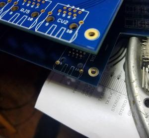
I have just been testing a new version of my four toggles PCB that does phantom, pad, mic/line and phase switching. It is the same schematic just with the switches arranged in a square instead of in a single column. To aid wiring up to it I had marked the hot pin on the 3 pin Molex connectors I use to connect mic, line and the output. Wired it up and odd things happened. Mic/line switch did nothing - mic signal still came through. 20dB pad did nothing but phase switch reduced level by about 6dB. Realised I had left some component soff the PCB. Fitted and retested - very similar results. I began to suspect I had made a mistake in the PCB layout so go back to computer and load up PCB layout onto screen. Carefully check all traces - nothing wrong. Peer at PCB layout for about half an hour and then it hits me. I had rotated connectors at some point to ease tracking but I had not moved the silk screen letter H used to indicate which pin was hot. The H was next to the screen pin!! Rewired the test PCB ignoring the 'H' and it all works perfectly.

Cheers

Ian
 
Thanks for sharing this Ian.  To quote your signature line: 'The only people not making mistakes are the people doing nothing'  Being able to share your mistakes so that others may learn from them is a noble character trait.  :)
 
If testing with phantom and an expensive mic could have been an expensive mistake...

Noted, check silk screen (and code comments)...

JS
 
joaquins said:
If testing with phantom and an expensive mic could have been an expensive mistake...

Noted, check silk screen (and code comments)...

JS

Been there, almost done that. I had a miss wired phantom connection on a PCB so phantom was always on. This blew up the op amp output stage of my test set - fortunately the manufacturer had included fuses for this so it was not as expensive as I first thought. SInce then the test set is always few via transformers.

Cheers

Ian
 
Take comfort you didn't recently make a PCB and forget to mirror the non-symmetrical part to bottom layer...

DAInIhJ.jpg
 
boji said:
Take comfort you didn't recently make a PCB and forget to mirror the non-symmetrical part to bottom layer...

DAInIhJ.jpg
I have done something similar. I designed a small PCB, about one inch square to make a right angled PCB socket for by  my new 35mm modules. I then designed a new version of my classic PCB, replacing the existing tube sockets with this new  right angled one. Somehow I got the holes on the PCB the wrong way round; 9 to 1 instead of 1 to 9.

Cheers

Ian
 
  On a quite bitchy board to self etch (as I still do as delay times here are prohibitive) I successfully etched a PCB containing an 0.5mm pitch 30 pin part, in the printing process the image got shrunk by  ~3%. Aligning the first pin with the first pad would make the last one to be on the space between the two pads, I'm about to re-etch the thing.
  I use toner transfer, but I got a laminator which makes things so much much better than the iron, I don't even think in going to photosensitive/exposure mess.

JS
 

Latest posts

Back
Top