jdbakker
Well-known member
EDIT 20090831:
Revision 1.2 uploaded. Seven transistors eliminated at the cost of ~1dB 3rd rise at 1kHz (but still ~-170dBc), otherwise no major spec changes.
EDIT 20090828:
Revision 1.1 uploaded. 3rd and higher are now 20dB lower, otherwise no major spec changes.
Original post:
[now it's ready to be posted]
Hi all,
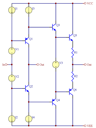
I've finished a first draft of the current-feedback op-amp that is to form the first stage of my discrete mic pre work-in-progress.
Have a look at the schematics. (EDIT 20090828: this is the original version).
Preliminary specs:
(running on +/- 24V supplies, driven by a 100R source, into a 100R load, set for an amplification of 21x (~26dB))
Noise figure: ~1.5dB
Dynamic range: ~130dB between 20Hz-20kHz noise floor and clipping
Output swing: +/-21V without load, +/-20V with 100R load
Slew rate: +40/-110 V/us
Distortion: rhymes-with-lies claims that with a 500mVRMS input signal at 1kHz the 2nd is at 128dB below the fundamental, and the 3rd and higher are 150dB down. At 10kHz those figures are 109dB and 130dB, respectively. I expect that in real life noise pickup and thermal distortion will dominate (never mind that I have no equipment to measure 300nV harmonics in the presence of a 10V fundamental...)
Frequency response: 3dB down (rel 26dB) at 6MHz, unity gain at 24MHz. Apart from 0.4dB in-band gain peaking the AC response is monotonically decreasing to 1GHz (I looked no further, and I expect anything over a few tens of MHz is going to be dominated by parasitics)
Overshoot when the amp is slew-limited is about 30% of the step response; recovery is within 1us. Negative clipping shows 300mV overshoot; no phase inversion or other funny business.
And yes, that's enough transistors to build two or three traditional DOAs.
My main problem in designing this monster was handling negative clipping. Contrary to voltage feedback designs where you know that the maximum current into your VAS stage is set by the differential pair tail current source, a current feedback op-amp will happily dump as much current into your negative input (and thus the VAS) as your feedback network impedance allows. For this design, that's about 100mA in differential configuration. I had to implement a three-stage clip control: D18/D20 work to keep Q4 out of saturation, with D20 bootstrapped by R6. Similarly, D21/D22 are a Baker-ish clamp for Q16, and for really serious overloads the drop across R11 drives input transistor Q1 into saturation.
This brings me to one of my worries: when Q1 saturates, its base current increases, changing the amplifier's input impedance. This may lead to...funky responses in a reactive source. How much good is it to build an amp that clips gracefully if it produces, say, ringing in a mike/cable assembly? Worse, what'll happen to a ribbon mic? Granted, for this to happen the ribbon mic would have to somehow send a >5V signal down the line, but still. I need your input here; if this is a real problem I could implement a simple current limiter around the input transistor, but that does increase distortion some.
I have considered a current source in place of R7. While this increases VAS impedance and open-loop gain and lowers distortion even further, higher order products become relatively more present. Besides, an active current source will have more noise than the present solution.
Samuel: thanks for the hint on getting better output Z for cascodes. Like you've said elsewhere VAS output current swing has a strong impact on VAS distortion, and your suggestions have helped a lot in that area.
The 2N4403 on the input is just a placeholder. If you feel you need that last bit of noise performance a 2SA970 or 2SB737 should work fine. I might try a FET to see what happens. For the rest of the small-signal transistors I would recommend the BC550C/560C over the '547C/557C.
The output drive is deliberately beefy to allow for a low-Z attenuator between this stage and the next one. There's no overcurrent protection yet, but I'm not sure that it's needed for something that always drives a known load (plus I'd be loathe to add two more diodes, that would make this design too complex).
And yes, that's a lot of diodes, but I've pencilled in duals in SOT-23. These are twice as fast to place (as there's only half as many), plus getting the orientation/polarity wrong on a 3-pin part is much harder than on a 2-pin part.
Like in regular power amps, I am considering feeding the output transistors from an unregulated supply.
I need to tweak the biasing for the cascoded diamond buffer some. Apropos cascodes: I've used them as much to isolate high-dissipation positions from transistors where the actual VBE matters (ie: the current sources). More apropos cascodes: I've found that it's time to stop tweaking and start publishing/building when you get the urge to start cascoding your cascodes.
Thoughts? Suggestions? Flames?
JD 'but where to buy that 1kF capacitor?' B.
Revision 1.2 uploaded. Seven transistors eliminated at the cost of ~1dB 3rd rise at 1kHz (but still ~-170dBc), otherwise no major spec changes.
EDIT 20090828:
Revision 1.1 uploaded. 3rd and higher are now 20dB lower, otherwise no major spec changes.
Original post:
[now it's ready to be posted]
Hi all,
I've finished a first draft of the current-feedback op-amp that is to form the first stage of my discrete mic pre work-in-progress.
Have a look at the schematics. (EDIT 20090828: this is the original version).
Preliminary specs:
(running on +/- 24V supplies, driven by a 100R source, into a 100R load, set for an amplification of 21x (~26dB))
Noise figure: ~1.5dB
Dynamic range: ~130dB between 20Hz-20kHz noise floor and clipping
Output swing: +/-21V without load, +/-20V with 100R load
Slew rate: +40/-110 V/us
Distortion: rhymes-with-lies claims that with a 500mVRMS input signal at 1kHz the 2nd is at 128dB below the fundamental, and the 3rd and higher are 150dB down. At 10kHz those figures are 109dB and 130dB, respectively. I expect that in real life noise pickup and thermal distortion will dominate (never mind that I have no equipment to measure 300nV harmonics in the presence of a 10V fundamental...)
Frequency response: 3dB down (rel 26dB) at 6MHz, unity gain at 24MHz. Apart from 0.4dB in-band gain peaking the AC response is monotonically decreasing to 1GHz (I looked no further, and I expect anything over a few tens of MHz is going to be dominated by parasitics)
Overshoot when the amp is slew-limited is about 30% of the step response; recovery is within 1us. Negative clipping shows 300mV overshoot; no phase inversion or other funny business.
And yes, that's enough transistors to build two or three traditional DOAs.
My main problem in designing this monster was handling negative clipping. Contrary to voltage feedback designs where you know that the maximum current into your VAS stage is set by the differential pair tail current source, a current feedback op-amp will happily dump as much current into your negative input (and thus the VAS) as your feedback network impedance allows. For this design, that's about 100mA in differential configuration. I had to implement a three-stage clip control: D18/D20 work to keep Q4 out of saturation, with D20 bootstrapped by R6. Similarly, D21/D22 are a Baker-ish clamp for Q16, and for really serious overloads the drop across R11 drives input transistor Q1 into saturation.
This brings me to one of my worries: when Q1 saturates, its base current increases, changing the amplifier's input impedance. This may lead to...funky responses in a reactive source. How much good is it to build an amp that clips gracefully if it produces, say, ringing in a mike/cable assembly? Worse, what'll happen to a ribbon mic? Granted, for this to happen the ribbon mic would have to somehow send a >5V signal down the line, but still. I need your input here; if this is a real problem I could implement a simple current limiter around the input transistor, but that does increase distortion some.
I have considered a current source in place of R7. While this increases VAS impedance and open-loop gain and lowers distortion even further, higher order products become relatively more present. Besides, an active current source will have more noise than the present solution.
Samuel: thanks for the hint on getting better output Z for cascodes. Like you've said elsewhere VAS output current swing has a strong impact on VAS distortion, and your suggestions have helped a lot in that area.
The 2N4403 on the input is just a placeholder. If you feel you need that last bit of noise performance a 2SA970 or 2SB737 should work fine. I might try a FET to see what happens. For the rest of the small-signal transistors I would recommend the BC550C/560C over the '547C/557C.
The output drive is deliberately beefy to allow for a low-Z attenuator between this stage and the next one. There's no overcurrent protection yet, but I'm not sure that it's needed for something that always drives a known load (plus I'd be loathe to add two more diodes, that would make this design too complex).
And yes, that's a lot of diodes, but I've pencilled in duals in SOT-23. These are twice as fast to place (as there's only half as many), plus getting the orientation/polarity wrong on a 3-pin part is much harder than on a 2-pin part.
Like in regular power amps, I am considering feeding the output transistors from an unregulated supply.
I need to tweak the biasing for the cascoded diamond buffer some. Apropos cascodes: I've used them as much to isolate high-dissipation positions from transistors where the actual VBE matters (ie: the current sources). More apropos cascodes: I've found that it's time to stop tweaking and start publishing/building when you get the urge to start cascoding your cascodes.
Thoughts? Suggestions? Flames?
JD 'but where to buy that 1kF capacitor?' B.