Behringer ADA8000 pre bypass questions

GroupDIY Audio Forum

Help Support GroupDIY Audio Forum:

This site may earn a commission from merchant affiliate links, including eBay, Amazon, and others.
Hi,
I'm trying them out with a RME MADI right now to a Soundtracs Topaz and the DA sounds quit acceptable.Clocking with a Swissonic WD8.
Didn't get the time yet to test the AD's.

Greets
 
The DA's are actually quite respectable. As for going into the 1/4 line, it works well also. Is it the end all, NO. I'm also looking to improve them some, but the way they are right now doesn't create me any problems. I know where I feel I need to compensate for them and I'm ok.
As my understanding goes right now, I haven't given it thorough thinking, If you take the balanced out of your pre and inject it into the tlo74 unbalanced it should work. You'll be giving up 6db right there by unbalancing, still have their V protection, and life will be ok. Again, I haven't tried it yet. I haven't had a meter with me to find out which wire is which going between the mother board anf front board.
If someone tells me which is which, or I remember to grab my meter and beep it out one of these days. I'll clip the wires and see what happens. I have no problem making mine a guinny pig, except time.

Michael
 
quote: "still have their V protection, "...

Just what is this V protection? The only schematic I've seen so far (from Gyraf, with disclaimers) doesn't have any explicit protection. Have I missed something? (entirely possible)
 
[quote author="MHanson"]
As my understanding goes right now, I haven't given it thorough thinking, If you take the balanced out of your pre and inject it into the tlo74 unbalanced it should work. You'll be giving up 6db right there by unbalancing, still have their V protection, and life will be ok. Again, I haven't tried it yet. I haven't had a meter with me to find out which wire is which going between the mother board anf front board.
If someone tells me which is which, or I remember to grab my meter and beep it out one of these days. I'll clip the wires and see what happens. I have no problem making mine a guinny pig, except time.

Michael[/quote]


michael,

very helpful post!! thanks for the offer!
the tl074 is a opamp, would it be ok injecting a hot signal in an opamp?

if you check out my first post, the first PDF link is a schematic of the front/main board pre section.
im really hoping we can get a halfway decent use out of this. of all the stuff ive heard from people these AD's are really decent. and the whole unit only cost me 180$, for eight channels. so id really like to make this a usuable piece.


thanks again man, good to have you here. if you could find out what you were thinking that would be awesome.

:thumb:
 
Vastly prefer the new Avatar---I find the animated ones very distracting. Sign of age perhaps.

"if you check out my first post, the first PDF link is a schematic of the front/main board pre section. "

That's the one I looked at, and I don't see any explicit protection other that a bit of attenuation. Maybe there are clamp diodes in the ADC and it's sufficient just to limit current via the resistors. Or maybe it counts on the intrinsic current limiting of the op amps. Were it not for the inverting amp complementing the signal from the preceding amp the common-mode signal could rise well above 5V and well below 0, which would be blasting the inputs of the ADC. BTW, unless there are internal coupling caps in the chip (unlikely) the 2.2M pulldown R's right at the ADC inputs don't make sense. I should think you would want those inputs to sit at the half-supply, in this case 2.5V, and I would suspect there are internal R's or their equivalent in switched capacitor structures to ensure that.
 
So as I think about it, a one-transistor phase splitter (!) would be all you would need to take your single-ended voltage and provide a balanced drive for the ADC. An R in the emitter and an R in the collector. Cap-couple out and set up voltages so that you can't get more than about 5V peak-to-peak out of the emitter. Have the little series R's to each ADC input and the cap across for the lowpass filtering. If the distortion is worrisome at peak signal use a Sziklai follower (a complementary pair with 100% feedback) in place of the single Q.

The power supply rails for the stage need to be quiet, especially at the collector, since there is essentially no power supply rejection.

This would only give you unity gain out of each of collector and emitter though, +6 dB balanced, so I'm not sure if that is enough for your anticipated input signals. The ADC datasheet says it handles 4V p-p at each input, and I guess that means for full scale digital. This would correspond to 4V p-p or 1.414V rms at your line-level input.
 
alot of that flew over my head :thumb:

tell me a little more about this idea, would the board need to be powered, a board for each channel?

like this?


ttl_input_phase_splitter.gif
 
asm I'll send you a schem if you will PM me with an email addy and you can post it (I'm still challenged in that regard). Meanwhile where did you get the symbol for a two-emitter transistor? That schematic resembles a TTL gate!

The pair connection I'm talking about is the upside-down version of half of the discrete portion of the existing schematic. Think of the PNP/NPN pair as a composite single transistor and use it as the active element in a phase splitter. Come to think of it the PNP input version would be fine as well. Some call this an accordion- or concertina-type phase splitter.

I did a sim last night and distortion is an acceptable <.02%, mostly mix of second and third, at 4V p-p in, 4V p-p out of each output, with a 1k source impedance. I'll have to add a couple of parts for proper input bias and coupling C, and something to reduce the rail to the needed ~10V for the overload protection scheme to work.
 
So that's why these are such a PITA about clipping at 0.
and yeah, the darn 1/4 is through the preamp too, tried that.
I've also noticed, that on mine, and I gonna get another just to
test, but it seems all of the right channles, 2,4,6,8 seems to be
a hair hotter than the odd 1,3,5,7.

I can see a 10db pad xlr/xlr connector? some came with my avocet
would those work, just variable pad's with female/male ends, that you'd use anywhere basiclly? I haven't cracked one, but it's just a passive pad I thought.. I am using them after the ssl compressor, I don't need then after the avocet because my adam's have gain adjustments...

Interesting.. I'd only need this on a couple of channels, but on some devices it would be nice to truely go out at digital 0 and then analog PAD, but what is truely the difference between analog attenuation and just turning it down digitally on the mixer 10db?

does this make sense?
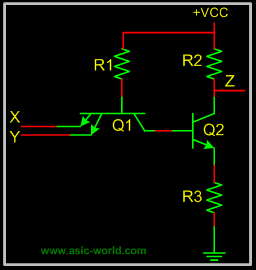
 
asm---thanks for posting. I guess some doctoring is needed to make all the lines show up properly---the connections seem to be missing between C5, R23 and into "INL-" on the ADC. But it should be pretty clear what's missing.

Brad
 
something kinda caught my eye and I'm wondering about it.. the protection diodes on the INL+ are in parallel.. I assume one of them is supposed to go to INL- instead? Also, how important are they right there after the coupling caps? I would think that they are more needed on the bases of the NPN/PNP pair, or at least another set of them there?

on another note, how are the ADC/DAC's grounding? I assume they have separate D and A grounds? are they grounded through ferrites? no sense in trying to upgrade the things if the boards were badly designed to begin with.

more on this later.. :thumb:
 
Ooops thanks for noticing that--drafting error there---you are correct they should be applied symmetrically.

If you are expecting great big input signals then it wouldn't hurt to have one diode reverse-biased across the NPN base-emitter.

I was most worried about sending the 1101 into latchup or other damage during turnon/off transients, hence the diodes. Ideally they should be schottkies as well, but I suspect 4148's will be adequate. As mentioned, if the supplies go up and down properly the diodes should not be required even under heavy overload at the input.

Wavefront claim that their part works fine with a single shared D and A ground---there is a link to the datasheet somewhere in this thread. Email addy is www.wavefront.com.

The impression I had was that asm et al. were doing a similar but not identical layout (see his remarks about the difficulty of soldering an SMD package), but perhaps that's incorrect.
 
[quote author="bcarso"]asm---thanks for posting. I guess some doctoring is needed to make all the lines show up properly---the connections seem to be missing between C5, R23 and into "INL-" on the ADC. But it should be pretty clear what's missing.

Brad[/quote]


i dont see any connections missing, when the image is resized (thumbnailed) it wont shot up some pixels (lines). just click on the image and make it big and see if it does the same thing still.
 
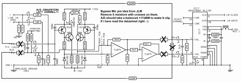
I haven't read all the thread but to bypass the mic pre remove 5 resistors and run two wires with 220r in each one to pin 2 & 3 on the XLR. The A/D should take a balanced +17dBM to clip if i have read the datasheet right :)

micprebypass.gif


Joe

www.jlmaudio.com
 
"If you are expecting great big input signals then it wouldn't hurt to have one diode reverse-biased across the NPN base-emitter. "

Yeah I was just wondering about that since I've had to do it before on other projects.

Wouldn't putting the protection on the PSU outputs for global protection be a little easier(maybe better?)? I'm not sure about Schottkys here either(unless you go for the expensive superfast ones).. guess it all depends on the transient that you get and how bad it is. maybe a couple TVS instead?

As for a shared D and A ground.. I'd have to see(and test the shit out of it..) it to believe it. I deal with mixed signal video all day and improperly mixed D and A grounds from the other engineers are the bane of my existence.. I have screamed and yelled and damn near cried trying to get them to do things correctly but noooooo... constantly having to go back and redesign crap that was "overlooked" during design. but i digress..

I actually prefer SMD stuff due to it's ease of prototyping and size. I guess i'm alone on that..

If anyone wants I can do a layout of a prototype input in SMD.

another question about these boards, are the ADC/DAC ICs driven by a MCU? if so, is it a specific code for these IC's or could it be modified for, lets say, the Crystal semi chips?
 

Latest posts

Back
Top