Can this be done on a PCB?

GroupDIY Audio Forum

Help Support GroupDIY Audio Forum:

This site may earn a commission from merchant affiliate links, including eBay, Amazon, and others.

skrasms

Well-known member
Joined
Jun 16, 2004
Messages
72
Location
Gary/Purdue-Lafayette
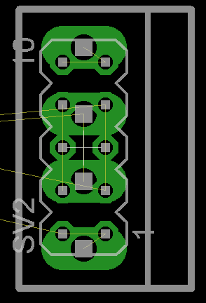
I ran into this issue today. The circuit can use either of two parts in a particular spot, and I want to include both without taking up a lot of extra board space. The problem is that there must be overlap of the pads and drill holes to make that possible. This picture shows what I'm going for:

pads.png


Can that be altered so that a board house can do it? Eagle PCB won't let me come close to it.
 
You can do routed slots. I have. you can even have them plated, if you want.

you could probably also do squares and triangles or any other shape, within reason. (well, also taking into account that corners will be rounded)

what you can't do is just 3 holes overlapping, because that is 3 separate drill down movements, and once the first hole is drilled, if you drill overlapping it, your bit will bend into the existing hole, and snap off.

so - you can't get exactly what you were looking to do, but try drawing what you want in the drill layer as lines, not just 3 overlapping holes.

oh, and if you want this to be a "pad" then while you're at it, you might have to get a bit creative with copper fills and solder mask layer gaps, too.

oh - and you should state in the PCB file exactly what you're trying to do - that way the PCB house's CAD engineer won't "fix" your PCB for you.
 
[quote author="no-fi"]
what you can't do is just 3 holes overlapping, because that is 3 separate drill down movements, and once the first hole is drilled, if you drill overlapping it, your bit will bend into the existing hole, and snap off.[/quote]

I don't think I was clear here. It doesn't have to be just 3 holes overlapping. If that shape was made into a plated triangle with rounded corners it would still work fine. That's why I asked if it could be altered to work. Eagle doesn't seem to support that in any way that I can find.
 
my simple workaround is, you can rotate your alternative parts by some different degrees than multiples of 90°, entering in Eagle command line something like
ROTATE R17 'C2'
to rotate your capacitor C2 (transformer or whatever) by an rotationangle of 17 degrees, route traces to the corresponding alternative part drillholes and be done with it.
There may be different/better approaches to solve this, but this works for me and some additional simple drillholes may end up cheaper.
-Harpo
 
[quote author="skrasms"]
I don't think I was clear here. It doesn't have to be just 3 holes overlapping. If that shape was made into a plated triangle with rounded corners it would still work fine. That's why I asked if it could be altered to work. Eagle doesn't seem to support that in any way that I can find.[/quote]

I can do random cutouts in protel, but i can't help you with eagle, cause I've never used that program.

does eagle have any "line" primitives you can draw? (similar to a section of track, but not associated with a net??) draw your line at the right thickness in the drill layer, and there you go. but DO explain in the PCB file exactly what you're doing, or you risk them doing it wrong.


why don't you just avoid the whole hassle, and its large chance for error, and just move the doepfer header to the right, so it's more in the area of the blacet/motm power connector's friction lock than its through hole pads?
 
[quote author="no-fi"][quote author="skrasms"]
I don't think I was clear here. It doesn't have to be just 3 holes overlapping. If that shape was made into a plated triangle with rounded corners it would still work fine. That's why I asked if it could be altered to work. Eagle doesn't seem to support that in any way that I can find.[/quote]

why don't you just avoid the whole hassle, and its large chance for error, and just move the doepfer header to the right, so it's more in the area of the blacet/motm power connector's friction lock than its through hole pads?[/quote]

Mostly I'm trying to take some approaches that force me to learn how to do more with layouts. What you said is what I will likely end up doing, since it only adds about 0.05 inches to the width. On the other hand, I've never had a situation where cutting out a new shape was beneficial for any reason so I'm trying to learn about methods and limitations in accomplishing it.
 
yeah it's always good to learn new stuff.

I haven't done much challenging PCB-wise since I've been in my current job (5 years! eek!) though I've had other things to learn so it's all good...
:)

Outside board profile routing, cutting anything other than standard drill holes in a panel of PCBs is pretty unusual. And will generally cost $$.

the application I had for plated slots was for fastening an RF shield onto a PCB.
 
PostPosted: Sat Nov 01, 2008 4:26 pm Post subject:
This is a screenshot of the two parts overlapped:


I want to get a "universal" footprint for Blacet/Doepfer power connectors

Why do you have to overlap... Is there not room to go side by side.?
 
Back
Top