


Bombyx mori
Member
- Joined
- Jun 24, 2017
- Messages
- 13
Hello,
Could you please, take a look at my schematic, i'm trying to isolate and symetize an unbalanced input.
I've forgotten the 100R and 100µF on the XLR outputs... ;D
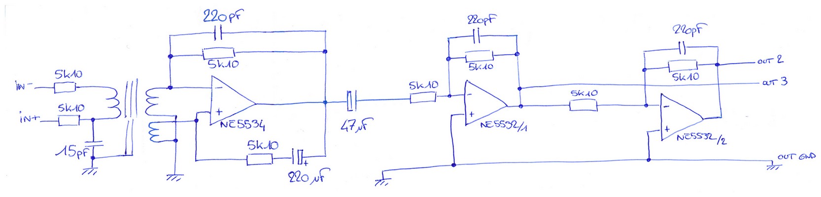
Could you please, take a look at my schematic, i'm trying to isolate and symetize an unbalanced input.
I've forgotten the 100R and 100µF on the XLR outputs... ;D


") )
)