Matador
Well-known member
So I decided that I wanted to do a micro controller-based curve tracer project to really exercise my acquisition of the following device:
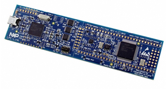
It's an LPCXpresso board with an integrated JTAG end-point and an LPC1769 target MCU. It runs at 120MHz and has the normal plethora of embodied peripherals like I2C and SPI. Most importably, it has support on-board for a LAN8720 ethernet phy, but more on that later. It's a great bargain for about $25!
So what I wanted to do is glue on to this board a basic ADC and DAC block, controlled over SPI. The DAC's would be used to provide test voltages to a Device Under Test (DUT), and then the ADC section would take voltage and current measurements which could then be displayed.
I selected the following chips for their simplicity, and given the fact that I have used them in previous designs so I know some of their quirks:
1) DAC - TI DAC7614: a quad, 12-bit voltage output DAC with SPI control
2) ADC - TI TLC2543: an 11 channel successive approximation ADC with SPI control
However the DAC chip can only source about 2mA of current, so I need a way to boost the current up to acceptable levels for small and medium signal BJT's and JFET's. I figure I need at least 100mA of output current in order to be useful.
I settled on the following circuit to take the DAC voltage output and buffer it for driving the device:
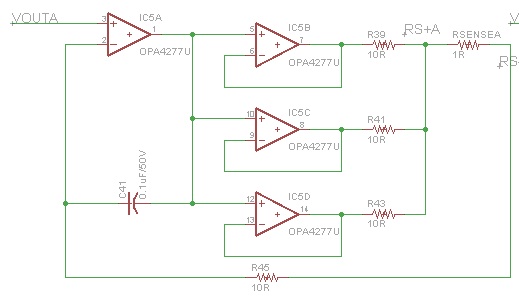
This is essentially a quad precision op-amp wired with three of it's active devices driving in parallel in a voltage follower configuration. According to the data sheet, this should be capable of driving 100mA before pooping out.
At the end of the feedback loop is a 1 ohm current sense resistor, the two terminals of which is taken to the following current sense circuit:
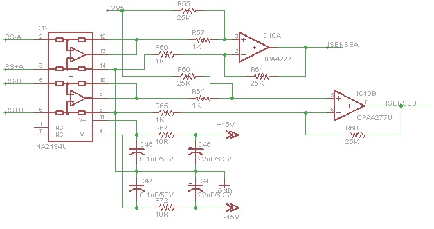
So this circuit is an INA2134 precision difference amplifier, followed by a bipolar to unipolar conversion stage. So the output of the difference amp is proportional to the current through the sense resistor (and negative for sink currents, positive for source currents), and the second stage afterwards level shifts this signal into a range of 0V to 5V (which is the VREF for the ADC stage). This voltage (along with the terminal voltage) is sampled by the ADC and should allow me to plot voltage and current for all channels as a function of input voltage.
So in order to control all of this: since this board contains an on-board ethernet PHY, all that's needed in the target schematic is an RJ-45 connector and magnetics. I'm planning on using a regular Magjack from Pulse.
I'm planning on using the FreeRTOS port of EasyWeb which contains support for a simple TCP/IP stack to have this all controlled via a web interface. Basically you can load a device into the board, load up the embedded server to control what kind of device is loaded, select the tests to run, then start the tests and display the results as a web page.
Since this MCU contains 512kB of code storage (as well as 64kB of SRAM), if I can, I'll port one of the open sources graphics libraries and generate bitmaps in real time (perhaps something like libgd). Any suggestions on this are welcome! This is so I can plot the IDS/VGS/VDS curves right on the web page. Barring that, I can export in Excel comma delimited format and make the curves that way, but if the web page can display the traces that would be even cooler.
Here's my prototype board layout (measures 4.5" x 6"):
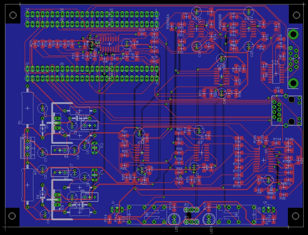
I have not broken up the ground planes yet, however given I won't be sampling at light speed I may be able to get away without breaking them up. I'll have to bread board it up and see how well it performs.
So I'll try to document all of this here in case anyone is interested in leveraging this MCU for other audio related projects like DAC's, ADC's, or perhaps preamp controllers or MIDI hosts/interpreters.
Suggestions and comments are always welcome!

It's an LPCXpresso board with an integrated JTAG end-point and an LPC1769 target MCU. It runs at 120MHz and has the normal plethora of embodied peripherals like I2C and SPI. Most importably, it has support on-board for a LAN8720 ethernet phy, but more on that later. It's a great bargain for about $25!
So what I wanted to do is glue on to this board a basic ADC and DAC block, controlled over SPI. The DAC's would be used to provide test voltages to a Device Under Test (DUT), and then the ADC section would take voltage and current measurements which could then be displayed.
I selected the following chips for their simplicity, and given the fact that I have used them in previous designs so I know some of their quirks:
1) DAC - TI DAC7614: a quad, 12-bit voltage output DAC with SPI control
2) ADC - TI TLC2543: an 11 channel successive approximation ADC with SPI control
However the DAC chip can only source about 2mA of current, so I need a way to boost the current up to acceptable levels for small and medium signal BJT's and JFET's. I figure I need at least 100mA of output current in order to be useful.
I settled on the following circuit to take the DAC voltage output and buffer it for driving the device:

This is essentially a quad precision op-amp wired with three of it's active devices driving in parallel in a voltage follower configuration. According to the data sheet, this should be capable of driving 100mA before pooping out.
At the end of the feedback loop is a 1 ohm current sense resistor, the two terminals of which is taken to the following current sense circuit:

So this circuit is an INA2134 precision difference amplifier, followed by a bipolar to unipolar conversion stage. So the output of the difference amp is proportional to the current through the sense resistor (and negative for sink currents, positive for source currents), and the second stage afterwards level shifts this signal into a range of 0V to 5V (which is the VREF for the ADC stage). This voltage (along with the terminal voltage) is sampled by the ADC and should allow me to plot voltage and current for all channels as a function of input voltage.
So in order to control all of this: since this board contains an on-board ethernet PHY, all that's needed in the target schematic is an RJ-45 connector and magnetics. I'm planning on using a regular Magjack from Pulse.
I'm planning on using the FreeRTOS port of EasyWeb which contains support for a simple TCP/IP stack to have this all controlled via a web interface. Basically you can load a device into the board, load up the embedded server to control what kind of device is loaded, select the tests to run, then start the tests and display the results as a web page.
Since this MCU contains 512kB of code storage (as well as 64kB of SRAM), if I can, I'll port one of the open sources graphics libraries and generate bitmaps in real time (perhaps something like libgd). Any suggestions on this are welcome! This is so I can plot the IDS/VGS/VDS curves right on the web page. Barring that, I can export in Excel comma delimited format and make the curves that way, but if the web page can display the traces that would be even cooler.
Here's my prototype board layout (measures 4.5" x 6"):

I have not broken up the ground planes yet, however given I won't be sampling at light speed I may be able to get away without breaking them up. I'll have to bread board it up and see how well it performs.
So I'll try to document all of this here in case anyone is interested in leveraging this MCU for other audio related projects like DAC's, ADC's, or perhaps preamp controllers or MIDI hosts/interpreters.
Suggestions and comments are always welcome!

