Bo Deadly
Well-known member
SOLVED?
I think I found the problem. The problem is that there is no problem. That wiggle in the modulation is actually normal.
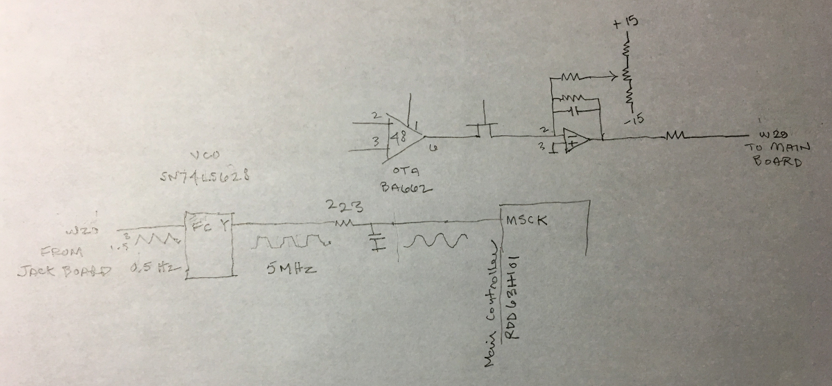
This type of digital delay adjusts the clock to just read audio straight out of ram faster or slower which makes it sound like the pitch changes. But it's using the same clock to write the data as well. Meaning the data is being written faster or slower which changes the pitch of the tone being recorded.
Fortunately I'm not really interested in playing tones through it.
UPDATE:
Here is a video but with sound so that you can actually hear the warble as it descends pitch:
Roland SDE-2500 Modulation Broken
and another, again a pure fixed tone, this time from the scope but looking at DOUT of the master controller (yellow) and the DAC output (blue):
Roland SDE-2500 Modulation Broken 2
So am I correct that the pitch modulation and clock should move exactly together. Maybe it's just hard to see on the scope? Is there some clever way to see the rate of change on the scope. Like XY plot with a fixed square or something?
--8<--
I got a very clean Roland SDE-2500 but the modulation is totally broken.
Here are "waterfall" FFT plots rotated 90 degress of a 440Hz tone through the SDE-2500:
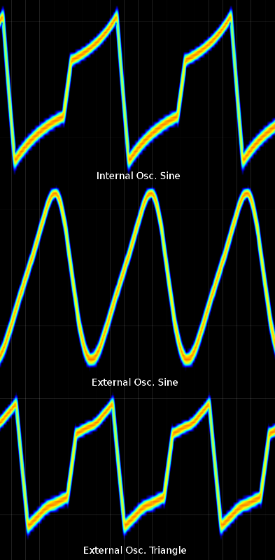
So the internal modulation is very broken. And even the external sine wave is pretty bad. The external triangle wave is worse.
Note: External Fn gen is an old Protek but makes very good LF waveforms.
Has anyone worked on this before? Does anyone have a manual?
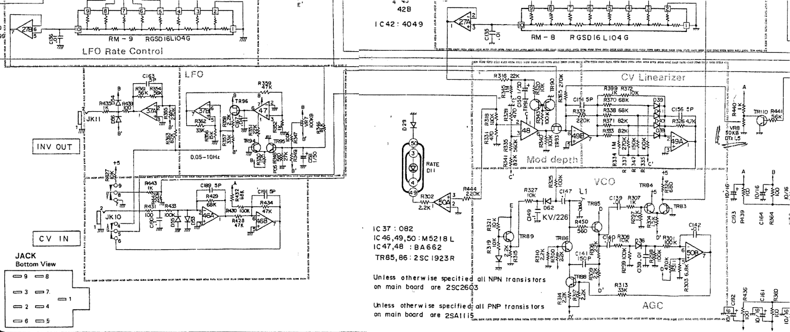
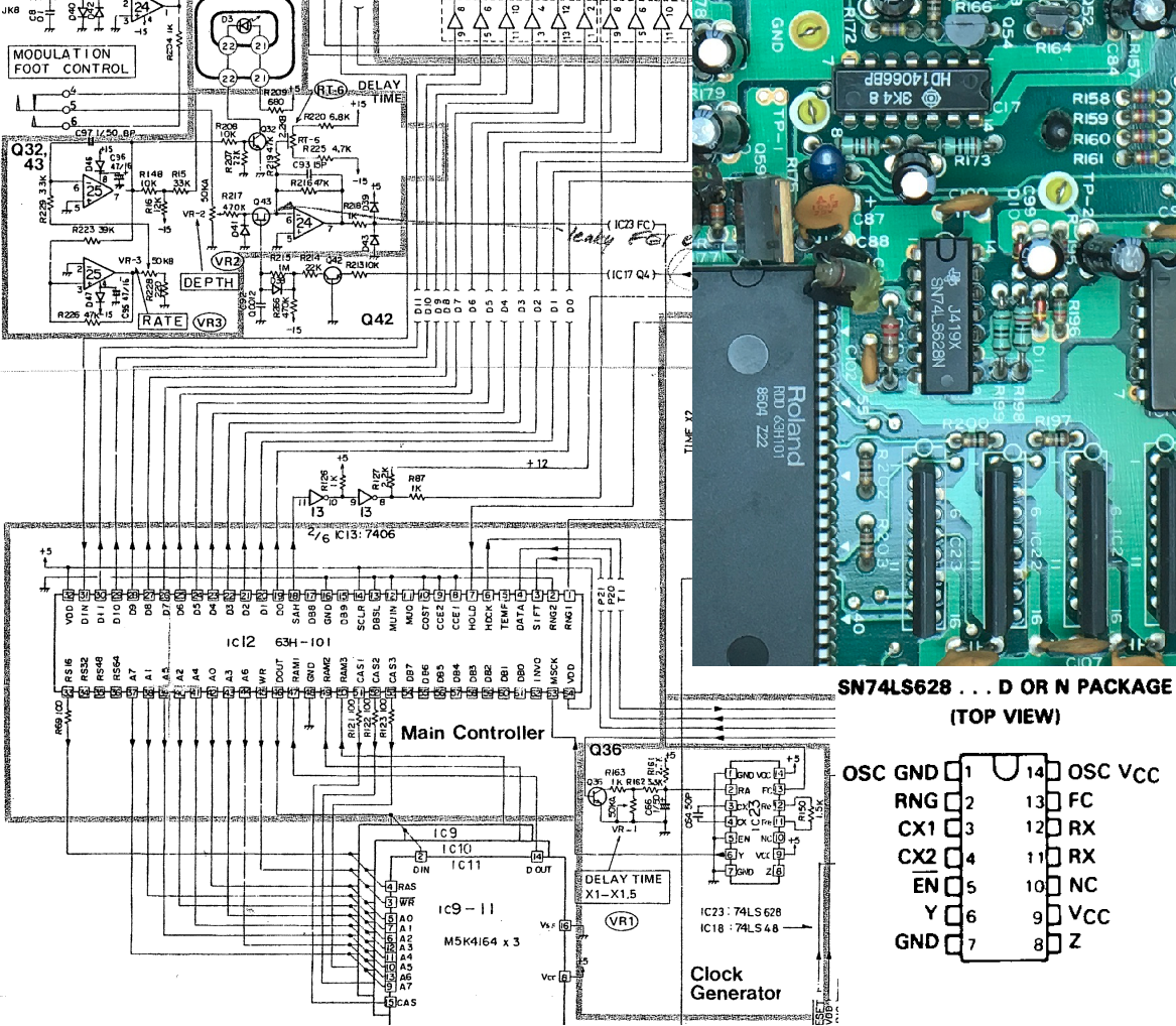
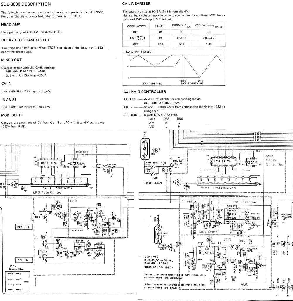
I found service manuals for the SDE-2000 and SDE-3000. Here are the interesting bits:
SDE-2000:

SDE-3000:
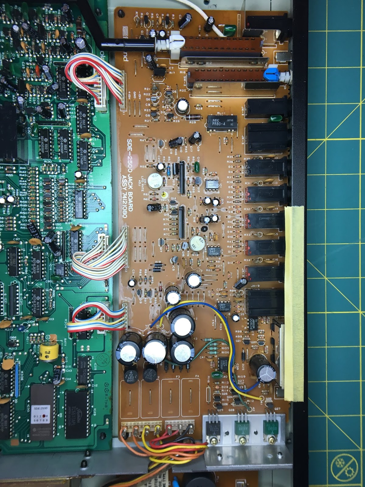
Just for posterity, here are closeups of the two main PCBs:
Board ASSY74121080
Warning: 4MB
Board ASSY74121100
Warning: 4MB
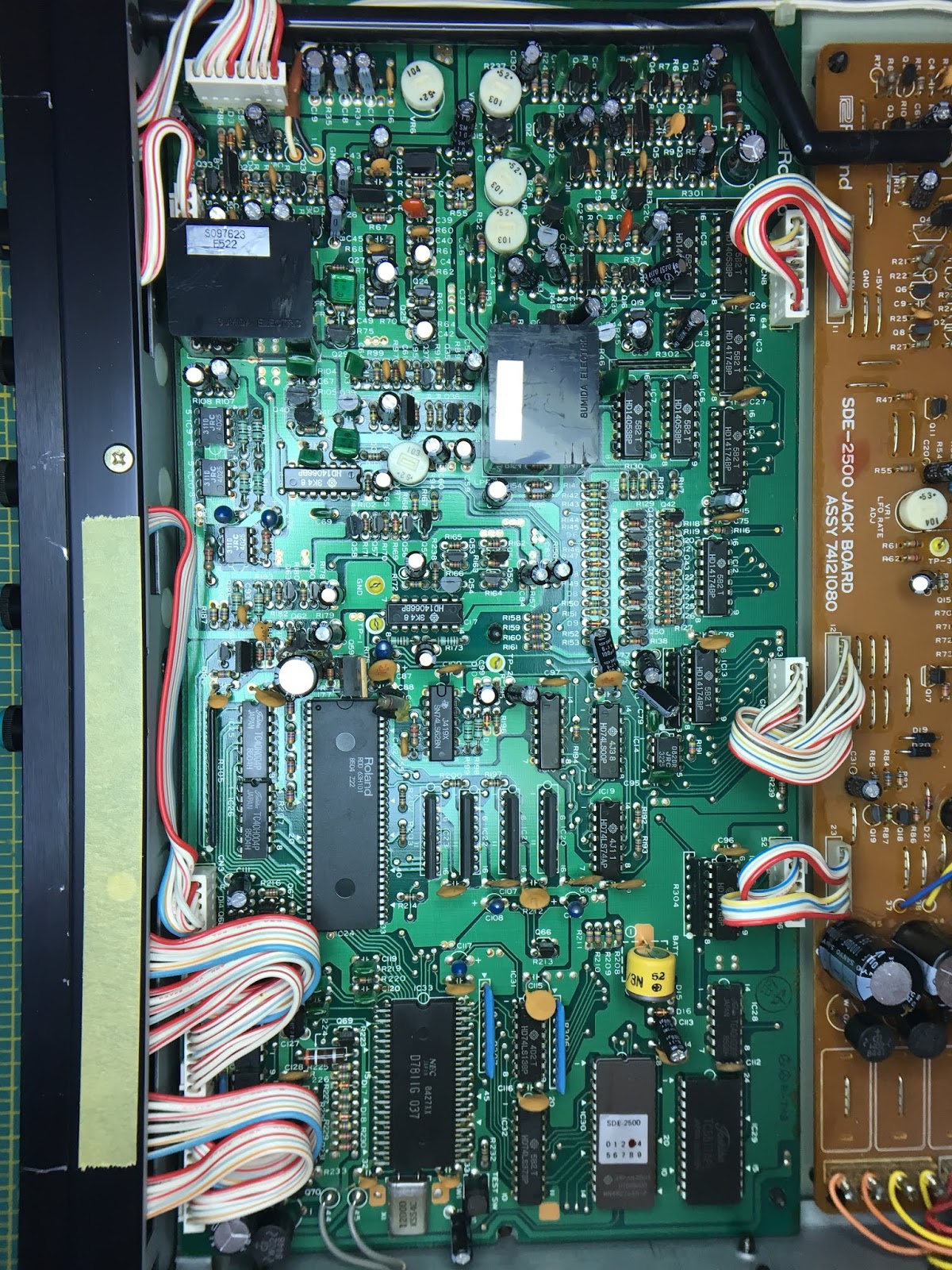
The SIP packages are BA662 OTAs which is a big clue as to where the relevant circuits are.
Any suggestions as to what the problem is and how to fix it?
I think I found the problem. The problem is that there is no problem. That wiggle in the modulation is actually normal.
This type of digital delay adjusts the clock to just read audio straight out of ram faster or slower which makes it sound like the pitch changes. But it's using the same clock to write the data as well. Meaning the data is being written faster or slower which changes the pitch of the tone being recorded.
Fortunately I'm not really interested in playing tones through it.
UPDATE:
Here is a video but with sound so that you can actually hear the warble as it descends pitch:
Roland SDE-2500 Modulation Broken
and another, again a pure fixed tone, this time from the scope but looking at DOUT of the master controller (yellow) and the DAC output (blue):
Roland SDE-2500 Modulation Broken 2
So am I correct that the pitch modulation and clock should move exactly together. Maybe it's just hard to see on the scope? Is there some clever way to see the rate of change on the scope. Like XY plot with a fixed square or something?
--8<--
I got a very clean Roland SDE-2500 but the modulation is totally broken.
Here are "waterfall" FFT plots rotated 90 degress of a 440Hz tone through the SDE-2500:

So the internal modulation is very broken. And even the external sine wave is pretty bad. The external triangle wave is worse.
Note: External Fn gen is an old Protek but makes very good LF waveforms.
Has anyone worked on this before? Does anyone have a manual?
I found service manuals for the SDE-2000 and SDE-3000. Here are the interesting bits:
SDE-2000:

SDE-3000:

Just for posterity, here are closeups of the two main PCBs:
Board ASSY74121080
Warning: 4MB

Board ASSY74121100
Warning: 4MB

The SIP packages are BA662 OTAs which is a big clue as to where the relevant circuits are.
Any suggestions as to what the problem is and how to fix it?


