PCB ground planes

GroupDIY Audio Forum

Help Support GroupDIY Audio Forum:

This site may earn a commission from merchant affiliate links, including eBay, Amazon, and others.
Etching copper off PCBs consumes reactive agents in the etchant. I've shared this before but PCB layout artists at Peavey were advised to leave as much copper on the boards as practical.
==
For some high current power amp traces, the solder mask was left off so extra solder would accumulate on the traces to lower the resistance.

JR
 
I am designing a few PCBs for tube preamps and would like to clarify some doubts regarding grounding and particularly the use of ground planes.
Other commercial and diy products I have seen use various solutions : star grounding, solid ground planes and even hatched ground planes.

I am keen to use a solid ground plane because it simplifies routing, but I have read that solid ground planes can be problematic for tube circuits, because of the high impedances at which tubes operate.
I am not sure this should be taken as a general rule of thumb since I am seeing many commercial products using a solid ground plane approach I guess it can be done with the right measures ?
Are there any specific considerations to keep in mind, for example isolation spacing between ground plane and signal traces, or sectioning the ground plane at specific points ?

I have designed the power supply section on a separate board, it's meant to be kind of an universal board that can power various tube circuits. It features HT output with simple crc filtering, unregulated DC for filaments and a section based on LM317 with a voltage doubler/tripler to get 48V for phantom power and a 12V/24V for relays and leds.
All the power supplies based on LM317 I have seen use a solid ground plane, whereas most tube power supply sections I found are without a ground plane, just using a star grounding approach.
Are there any reasons to avoid a ground plane in a tube power supply section ?
1. The ground planes (GP) on top layer are applicable, but they should not be connected with circuit ground (0V) on PCB. The ground plane should be connected to chassis (enclosure) at PCB corners. In such case it works as HF screen.
2. More applicable are hatched ground planes - such solution reduces parasitic capacitance with signal traces.
3. Separated GP for each stage of preamp - also useful decision.
4. Power supply doesn't requires GP, but this doesn't deny the presence of them.
5. Loss of treble - belongs to tales for kids.

example Guitar Preamp | Diyhifiaudio
 
when I was managing Mixer engineering for Peavey I would meet with the service department repair techs once a month and they would tell me emphatically what they were seeing on their repair benches.

JR

And what were the failures you saw most? I’d imagine mostly mechanicals/switches/the usual suspects vs your example of the lone underspec’d component as electrically designs were probably relatively well vetted and stable?
 
And what were the failures you saw most? I’d imagine mostly mechanicals/switches/the usual suspects vs your example of the lone underspec’d component as electrically designs were probably relatively well vetted and stable?
In 15 years I saw plenty. My sessions with the service repair techs was looking for possible design flaws, and to keep them happy.

I described multiple production problems. When using millions of components a year there are many opportunities for bumpy production.

I've shared several anecdotes about major component problems.

1-Notable was a large electrolytic capacitor used as a power supply reservoir cap. The manufacturer's swage tool (the mechanical attachment of the cap lead to the foil) broke. The swages were weak but most capacitors appeared to work properly. I was lucky to find this one early because a technician doing random incoming inspection called me about some outlier measurements. They were 1000 uF caps and several with bad swages were measuring tens of nF. The tech called me to ask if that was OK... I said let me check them. I took a few caps apart and found the weak lead swage. This was a common widely used component, so by the time I discovered the fault thousands had been used in production. I even had to recall one shipping container with suspect parts that was heading to a boat. I notified the manufacturer and they almost immediately found the fault and shut down their factory. This was a messy recall with a bunch of finished goods pulled from the warehouse for rework.

2- A similar problem on that scale was an problem with brittle potentiometer substates (the back side of a pot). The resistive element is carbon ink screened onto the back substrate. I called a vendor in to deal with too many pots breaking (substrate cracking) during manual insertion into the mixer PCBs. It turns out the American pot manufacturer had moved their production from Taiwan to China and they lost the recipe. The finished resistance can be pulled or tweaked several percent by cooking the pot substrates longer. I discovered that the new process manager was out of tolerance with the green resistance of the carbon ink, and cooked the substrates too long trying to get the bulk resistance in spec. The excessive over cooking make the pots brittle resulting in excessing factory insertion failures. Amusing or not, that vendor actually dropped Peavey as a customer. He said we were too picky. :rolleyes: When you are buying millions of pots a year there is usually a line of vendors waiting to sell us parts that don't suck.


There's more, large scale production reveals the weak sisters.

JR
 
Last edited:
1. The ground planes (GP) on top layer are applicable, but they should not be connected with circuit ground (0V) on PCB. The ground plane should be connected to chassis (enclosure) at PCB corners. In such case it works as HF screen.
Correct for RF applications, not so much for audio range.
3. Separated GP for each stage of preamp - also useful decision.
What's the point if they are connected to chassis?
2. More applicable are hatched ground planes - such solution reduces parasitic capacitance with signal traces.

5. Loss of treble - belongs to tales for kids.
Aren't points 5 and in contradiction?
 
Hatching (grid pattern) of ground planes allows 'thermal relief' which can/will prevent the ground area bubbling up when flow soldering the board when the copper expands and the 'glue' that holds the copper to the board surface softens. I suppose thoughtful application(design) of the apertures can fine tune the effects. All in all a great discussion so far with many small details coming up. For all the bashing that AMEK got from some Americans they did get many things 'right'. Pots on front panels almost always had reinforcing brackets or at least sufficient number placed to prevent pot damage or circuit connections cracking. Sometimes component manufacturers (I am thinking pots here) can 'lose their way' when situations change. Vishay 'bought' Sfernice who I think were the original manufacture of the little white pots that were used by Neve and many others in the 1970's. Following the sale to Vishay there was a noticeable change in the quality of the pots seen around 1990. In contrast the little green ALPS pots were incredibly reliable when there was only one known 'dailure point that was 'regular', which was actually a mechanical fault caused by failing to punch a hole for the anti rotation bump on the pot, meaning that when it was bolted up to the (ONE) panel (monitor level on an Angela2) after a month or two of operation either the left or right signal (I forget which but it was consistent) would become intermittent because of the stress caused by not sitting 'flat' on the panel.
In the realm of guitar amps it used to be said the pots should be wired to circuit boards simply because it allowed a degree of flexibility which is needed on gear that is thrown around and thermally cycled. Star grounding is yet another double edged sword. Great when the most prominent 'interference' was mains frequency and low harmonics but with everyone carrying a microwave transmitter in their pocket these days where a few inches of conductor are a handy aerial the situation is rather different. Unless some spectacular engineering design skills are employed, the old 'balanced audio' concept falls apart for frequencies above a few tens of KHz. In the 'good' old days equipment reviewers /manufacturers would publish the graphs of Common mode rejection (balance) where a healthy -70 dB or so at a couple of hundred Hz would degrade to 30 dB or so at 30KHz and presumably get a lot worse above that. Actually the roll off of the audio circuits would mask the 'failing' common mode rejection and it would be assumed to be benign because it wasn't necessarily appearing at the 'output' of the unit (whatever it was). Yes stuffing high levels at 50KHz WILL fry your tweeters when using your super wideband power amp.
 
Beatnik, I have a few general comments.

Try and appreciate how you would desolder and replace failed parts, and whether that would be easy rework or damage the pcb. With pads going directly to the gnd plane then avoid pads that can easily lift (such as a small pad on the other side of the board), or a pad where perhaps only 2 or three links are made to the plane for thermal relief but nearby parts/pads make it inconvenient to use the normal 4 links, and keep the link width substantial.

Also try and appreciate the main signal current path as a loop around the stage, with the local decoupling e-cap pads as the nodal link to other stages. For example, your layout in post #18 has a major signal current loop through the LL1680 primary, where the cathode 0V node should link to the local e-cap neg, and that e-cap neg pad should then link to other circuitry. That thinking may avoid unintentional parasitic coupling between stages.

An additional way of alleviating parasitic coupling is to appreciate if part spacing above the pcb surface can be a benefit, especially for coupling caps in a circuit that by design requires stable, repeatable and high frequency roll-off.

Consider whether any pad is connected to a lead with a relatively high temp, or the part itself is close to the pcb, or the part could get hot for a common failure mechanism. It is not uncommon to see temperature stressed traces or pcb regions, or even pads that have had solder melted from them in some equipment. Sometimes the use of a larger pad, or reserve a nearby small plane, can act as additional heatsinking.

Think about whether any traces related to high impedance node connections could benefit from shield/guard traces run along their length.
 
Last edited:
Star groun is a notion based on safety. It is definitely not the best solution for low-noise electronics, compared to hierarchical ground.
However, most tube circuits are low-current, even a 100W tube power amp operates with less than 500mA, except heaters. However heaters are a separate circuit, which is easy to make sure their current does not pollute the other parts. With such low currents, a rather flimsy ground circuit would still offer good performance, but nothing justifies makinf star ground a preferred choice.
I've had demonstrably good results with star grounding. Keeping current return paths to a star point along with the ground reference for the B+ regulators keeps the B+ clean to every stage, reduces stage to stage cross talk - a ground is an input to every stage, and improves, WAIT FOR IT!!! . . . . soundstage depth and imaging.

And if you want to poo poo star grounds, where do you want the charging current to the filter to go?
Not on any circuit return. I've serviced and modified enough hi end audio brands that have made this mistake and there is sawtooth hum in the output. Not good.
I believe the name "star ground" elicits grandeur, and allows its heralds to stand up, but really they should know it's good for safety, and poor for noise and other aspects of performance. Does one really want all their connections to ground going back and forth through lengths of wire?
Explain how it is poor for noise inside equipment.
A. Not going back and forth. DC goes one way - home.
B. Do you have a better way to route returns? Every stage's ground is supposed to be a zero point.

Chassis ground lugs can be a problem, too if you're wiring point to point. Over time they corrode and you have no control on chassis currents, especially near power transformers. In the good old All American 5 tube radio of the 40-60s you could get away with it because no one probably cared when listening on a 4" speaker.
I believe it's a manufacturing decision, that avoids creating large blobs of solder after wave soldering.

Maybe I misunderstand you. Does hatch mean "allowed to be crossed by other tracks"? In that case, that would be a wise decision, it it allows separating grounds that are not supposed to be mixed.

Don't overestimate the value of shielding. Indeed sensitive nodes need to be protected, but remember that the most important shielding is the one done by the case/chassis.
It depends on what you are shielding from what's radiating. You have to weigh the good and bad here. Shielding a hi Z circuit introduces capacitance to ground and shorts out hi freq. You can use a driven shield which you may want to research which keeps the driven shield at the same potential as the signal you're going to use. And if doesn't need shielding so much the better. If you're not worried about production costs in high qty and you are hand soldering you should do what's best for the design performance.
Not too long ago (1970's), ground planes were almost unknown in audio equipment. Many brilliant pieces of equipment had single-sided PCB's. Perhaps the most significant reason for adopting ground planes in audio circuits is because it reduces chemical waste.
Actually the Brits were conscious of that and adopted a style of layout that left most of the copper intact.
Yes there are brilliant designs but careful routing helped make them so, especially in noise sensitive equipment like an ACVM that measures in the microvolt range, Scopes, audio etc. Some were great just by dumb luck.
DC heaters do not radiate AC, so tehy can be routed almost any old way.
Yes BUT give the heaters an independent ground return to their supply. This keeps noise from DC regulators or residual hum out of the audio grounding. 7812s are not that quiet. The current is enough make noise voltage in the return line. I've never gone wrong separating the 2 supplies and connecting them to each other at the filter neg terminal of the filter caps.
Yes because twisted pairs reduce magnetic radiation.
You're correct but they also can capacitively couple to a hi impedance line, like the input of a hi gain phono or mic/instrument pre. DC regulated and well filtered to microvolts of residual noise is a better way to go. If you plan on AC tightly twist the wires together and route them as far from the input and hi Z lines as possible.
 
I've had demonstrably good results with star grounding. Keeping current return paths to a star point along with the ground reference for the B+ regulators keeps the B+ clean to every stage, reduces stage to stage cross talk - a ground is an input to every stage, and improves, WAIT FOR IT!!! . . . . soundstage depth and imaging.
Tell me how circuit A can be better than circuit B.
The current drawn by each stage create voltages between stages. Signal reference has to go through these small resistances and colect these voltages. With hierarchical ground these voltages are minimized by creating a very short and direct path for signal. It's been long known as "signal follows ground".
And if you want to poo poo star grounds, where do you want the charging current to the filter to go?
I believe you mean the reservoir capacitors currents? Where do they go? Read Kirchoff. They don't need a ground for closing the loop.
Not on any circuit return. I've serviced and modified enough hi end audio brands that have made this mistake
What mistake?
Explain how it is poor for noise inside equipment.
A. Not going back and forth. DC goes one way - home.
Profound misunderstanding. DC (as well as AC) has no home. Current exists in a loop. In taht respect, all points of teh loop are of equal importance. Calling one ground, or reference, or whatever, is a useful convention for circuit analysis.
B. Do you have a better way to route returns?
Hierarchical ground, of course.
Every stage's ground is supposed to be a zero point.
Doesn't make sense to me. Because of resistances introduced by wiring, and circulating currents, nothing is a "zero point". It's an abstraction, but when dealing with noise you can't rely on t, you have to consider all parasitics.
Chassis ground lugs can be a problem, too if you're wiring point to point. Over time they corrode and you have no control on chassis currents, especially near power transformers.
That's why chassis should never be used as an "audio ground". And for teh same reason, a dedicated ground should not make loops.
In the good old All American 5 tube radio of the 40-60s you could get away with it because no one probably cared when listening on a 4" speaker.
Correct. Same for many guitar amps, because guitar players have always been used to hum and buzz. The balance between the bonus of extra volume and the nusance of noise is still positive.
You can use a driven shield which you may want to research
I don't need to research it. As I explained in another post, I used it to carry an unbalanced signal with an impedance of 200 ohms across several kilometers of cable.
Yes BUT give the heaters an independent ground return to their supply.
Of course, currents should be separated as much as possible.
You're correct but they also can capacitively couple to a hi impedance line, like the input of a hi gain phono or mic/instrument pre. DC regulated and well filtered to microvolts of residual noise is a better way to go. If you plan on AC tightly twist the wires together and route them as far from the input and hi Z lines as possible.
There's no doubt DC heaters are the best choice for low noise. It depends on the expected level of noise performance.
However I've seen poor implementations of DC heaters where incorrect filtering resulted in increased buzz compared to AC heaters. 50/60 cycles doesn't coupled too well capacitively, but their harmonics do.
 
And if you want to poo poo star grounds, where do you want the charging current to the filter to go?
21-300x223.jpg


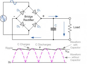
Here is a diagram of a FW rectifier and filter cap, and nothing is labelled ground. So where does the charging current go? Doesn't it return back to the voltage source (AC voltage in this case, or more typically back through the secondary windings), regardless of which node has the label "GND" applied to it?

I can label the top of the cap GND, and then the bottom of the cap would be negative wrt. that label, or I can label the bottom of the cap GND, and the top would be positive wrt. that label, but in all cases, current returns back to the source, does it not?

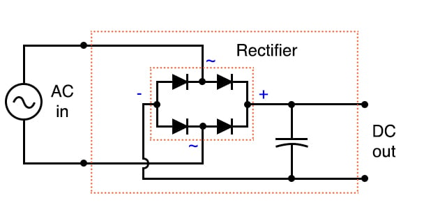
Here is another (identical) image:

rectifier-filter-circuit-schematic-diagram-1.jpg


So current leaves the top wire of the "DC out" section, flows through all of the magical shit inside the box, and returns back through the bottom wire. None of these are labeled "GND" either, and no star is involved.
This is a well known issue to anyone who has designed power supplies. To help visualize imagine 1 ohm resistors, instead of each PCB trace segment. There will be significant charging voltage artifacts caused by IxR voltage drops. So all of the traces to the left of the reservoir cap will have charging current artifacts superimposed on them. The traces to the right of the reservoir cap will only be modulated by the circuit draw (typically clean DC).

For power supply design it is important to connect the voltage regulator ground reference to a clean ground typically right at the capacitor bottom lead.

JR
 
Screenshot 2023-05-16 at 1.27.11 PM.png
This is how I've been doing tube amplifiers for the past few years, and there is no star ground. There is a safety bond at the IEC to the chassis, and a single connection between "0V" and the chassis right where the input jack is mounted to the enclosure. In fact, the amplifier will work just fine even without any bonding to the chassis and 0V, although noise is increased. This hierarchal scheme, coupled with heater elevation, has yielded some of the quietest amp's I've ever built.
 
Matador, that is a local star arrangement, which works well if there is no significant parasitic coupling from the PSU (or power amp for that matter) to the chassis - which could arise from local stray capacitances to chassis or a larger loop through the psu to mains and back around.
 
How so? Is it maybe a terminology issue on my part?

Anytime someone refers to 'star ground', I picture individual wires from each section/module/etc leading back to a common point, which is often recommended to be where the IEC safety earth is strapped.

RG. Keen's article describes it exactly this way:

RG Keen said:
One certain answer is star grounding. It's not the only way, but it's probably the only slam-dunk, cookbook way to ensure that if you start doing this, you will eventually have as low a hum as you can.
...
Simply put, star grounding means that you designate some special terminal as the "Star Ground" for the system. All other "grounds" will be referred to this one point. Then *every single place* that is connected to ground in the whole box has its own separate wire run to the Star Ground point. The ground wires radiate away from the Star Ground in all directions, hence the name. This has the unfortunate result that you may have a HUGE number of wires coming into the Star Ground point. Very hard to wire, just because of the large number of wires.

In my circuits, ground flows continuously, much like this picture of a 2203 marshall amp board I did, branching off to individual ground points as it follows the signal. The pour on the left side encompasses the connections between the main filter cap(s) and the center tap of the power transformer secondary. The chassis tie point is on the right, where the input jack resides.

Maybe in a compact chassis the difference is splitting hairs across a few tenths of an ohm?

344604103_922868515592214_3439387354826841123_n.png
 
Matador, that is a local star arrangement,
Which is as moronic as solid-state tube equipment.
which works well if there is no significant parasitic coupling from the PSU (or power amp for that matter) to the chassis
As there shouldn't be. Hierarchical ground arrangement formally precludes parasitic loops.
- which could arise from local stray capacitances to chassis or a larger loop through the psu to mains and back around.
Please explain how would star ground prevent that to happen.
 
In many situations, no ground scheme removes all noise path ground loops. Perhaps a common situation is the psu with a transformer, where parasitic capacitances from the dc rail can couple to chassis through the transformer secondary winding capacitance to core, and also couple to mains through the transformer secondary to primary winding capacitance. Those parasitic current paths form ground loops to the secondary side audio circuitry that return via the protective earth and the chassis and even external signal connections.

My reference to a local star arrangement relates to each functional block of the sld in post #35 having its own star ground - ie. there is a single trace link between the local star point of say the EQ and the power amp functional blocks. Another tag for that would be a distributed star arrangement. Same applies for how some circuitry on a pcb has its own local 0V ground pour, with only a single link to other 0V pours on the pcb. Same applies for 1950's audio amp circuitry where each valve stage has its own local star 0V (where cathode resistor and decoupling cap meet the stage B+ decoupling cap and input grid leak resistor and any screen decoupling).
 
In many situations, no ground scheme removes all noise path ground loops. Perhaps a common situation is the psu with a transformer, where parasitic capacitances from the dc rail can couple to chassis through the transformer secondary winding capacitance to core, and also couple to mains through the transformer secondary to primary winding capacitance. Those parasitic current paths form ground loops to the secondary side audio circuitry that return via the protective earth and the chassis and even external signal connections.
Describe how these currents circulate and how star grounding would make a difference.
My reference to a local star arrangement relates to each functional block of the sld in post #35 having its own star ground - ie. there is a single trace link between the local star point of say the EQ and the power amp functional blocks. Another tag for that would be a distributed star arrangement. Same applies for how some circuitry on a pcb has its own local 0V ground pour, with only a single link to other 0V pours on the pcb. Same applies for 1950's audio amp circuitry where each valve stage has its own local star 0V (where cathode resistor and decoupling cap meet the stage B+ decoupling cap and input grid leak resistor and any screen decoupling).
I guess many of us know what a star ground is, but I'm at loss about a "local star ground" or a distributed star arrangement." One is moronic antinomic, the other is pleonastic.
 
Last edited:
Back
Top