Implementing FET Switch

GroupDIY Audio Forum

Help Support GroupDIY Audio Forum:

This site may earn a commission from merchant affiliate links, including eBay, Amazon, and others.

Samuel Groner

Well-known member
Joined
Aug 19, 2004
Messages
2,940
Location
Zürich, Switzerland
Hi

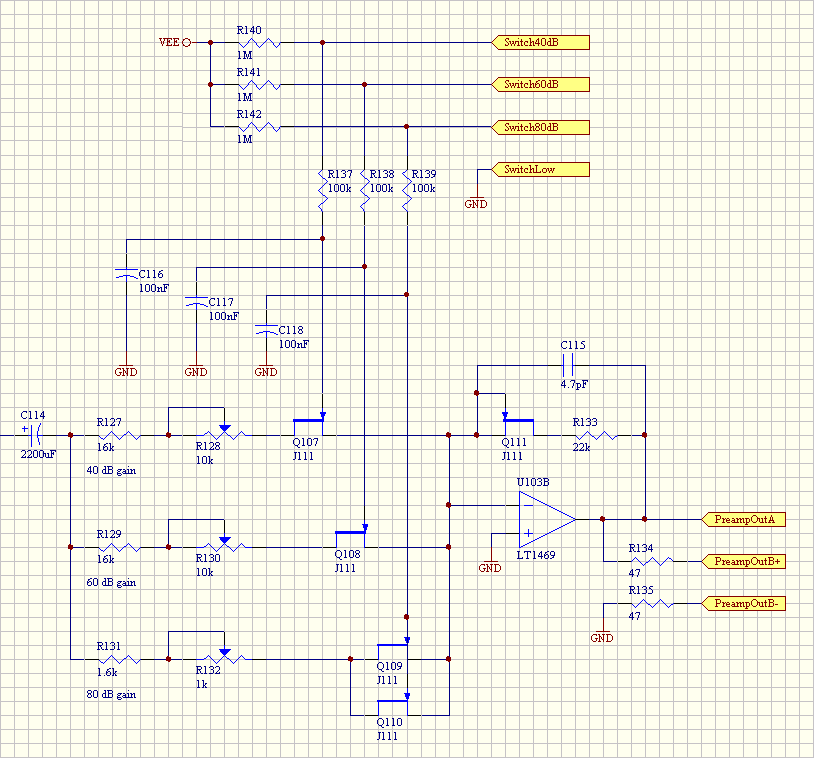
First time I use a FET switch so I have a few Qs. Application is a noise measurement amplifier, so distortion is not important but gain stability with temperature and age is. The current schematic:

fet_switch.gif


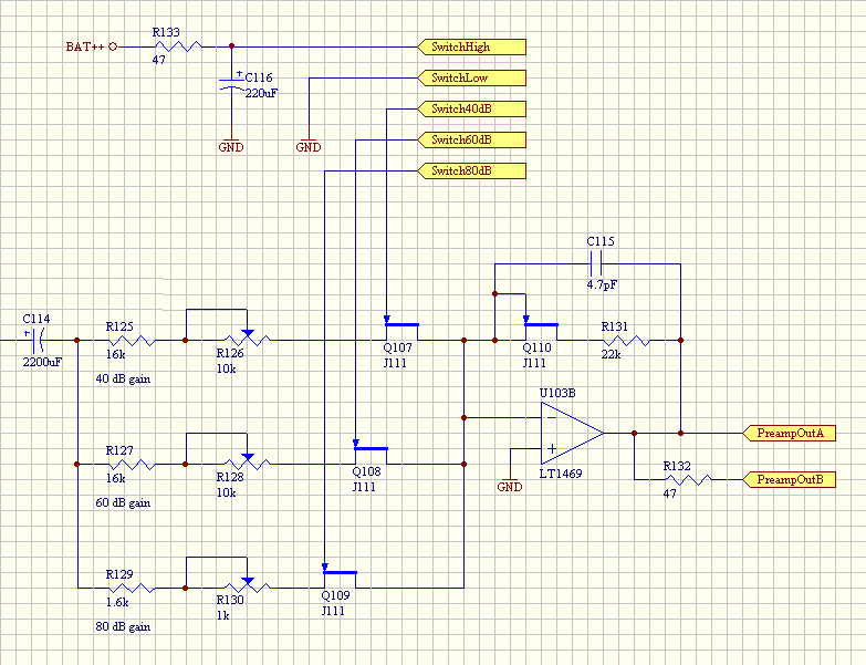
The gain stage shown is preceded by a low-noise differential amplifier with 40 dB or 60 dB gain, switched by a 3-position rotary switch which switches the FET gates as well. The second stage as shown in the schematic provides gain calibration and additional 20 dB gain for an overall gain of 40 dB, 60 dB or 80 dB. Maximum level at the opamp's output is 14 Vpp.

And now the questions:
* Is the FET choice a good one? Just what I have ready with low Ron.
* How high shall I pull the gates for off? I have 3.3 V, 9 V and 18 V ready. Simulation indicates that 18 V shows best offness (although this is uncritical here), so I'd use this if there is no further drawback.
* As the gain switch of the first stage and the gate switching is mounted on the same switch, I'm somewhat concerned about capacitive coupling of these stages. How critical is this? Do I need to RC-filter close to the gates?

Thanks for your help!

Samuel
 
[quote author="Samuel Groner"]* Is the FET choice a good one? Just what I have ready with low Ron.[/quote]
FWIW, Douglas Self had two nice EW+WW articles about switching:

Analogue Switching: Part 1 Jan 2004,
Analogue Switching: Part 2 Feb 2004

... but IIRIC main emphasis was on switching-transients, which may not be relevant for you.
He did gave some FET-type suggestions though, among them the type you used.
Can look it up but you'll have already done some R_on browsing yourself I assume.

What R_on values are you getting for the J111 ? If still relatively high w.r.t. the series resistor the obvious thing to do is to put some more in // (for Q109) to keep a decent R_on-cancellation for the gain.

If offness is still a concern other switching topologies could be used.

Regards,

Peter
 
A design technique that I used in a console back in the early '80s was to put the switching element in series between the - input of the opamp and the node connecting inputs and individual feedback resistors. By moving the switch element from the actual feedback network inside the feedback loop dramatically reduces it's contribution to nonlinearity. When I used this approach, I couldn't measure any distortion introduced by the switching (with circa '80s test gear).

To maintain stability with all switches open, a high value resistor always present from output to - input is useful to provide DC path. To reduce crosstalk, additional switches, shunting the unselected nodes to ground prevent any capacitive coupling through open switches.

This may be better performance than you want or need.

Switching J-fets in that topology I mentioned is a little easier than your approach since they are sitting at or near ground. You need to at least swap around the drain and source on your three input switches. The next consideration is how much input swing will you experience? The gate pinch off voltage is wrt both the drain and source, so if input swings to -15V, and so the drain (source as you've drawn it) of your not selected devices, the gate needs to be adequately lower than that -15V to prevent conduction.

A cheap and dirty fix for that is to just put diode clamps, or resistors to ground at those points to keep floating drain voltages clamped to +/- .5V or closer to ground. The diodes would be high impedance when switch closed and that node held to virtual earth by opamp, resistors would add noise gain, but no gain error. Then gate drive could be simply -15v with little concern of exceeding device breakdown.

For simple instrumentation using CMOS transfer gates (4016/4066) is pretty popular and might be easier.

JR
 
[quote author="mediatechnology"]Samuel: SSL often used this circuit with the J112. Not shown are the 10M resistors in series with the FET's gate:

SSL_J112_FET_Driver.jpg
[/quote]

You do get a slightly lower on resistance by forward biasing the gate diode, but that gate diode current needs to go somewhere, so may be undesirable in audio switching circuits, where the source is not grounded. A 10M in series will keep that current modest but not zero. Connecting the gate through a high value resistor to ground, with say a open collector pull down to -V should give an adequate on/off switching characteristic and no gate current. Many JFETs exhibit adequate conduction at 0 Vgs for high impedance switching.

For grounded mutes, the stray uA into ground is not a problem and fair trade for more kill. YMMV

JR
 
That is a little simplified but basically it. I used a high value R across opamp so there was always feedback present during switching or opamp would peg to a rail with no feedback.

I don't recall seeing this in print. I came up with my version late 70's/early '80s, for a console to electronically switch an entire bank of channels between tracking and mixdown. but the ancients are always stealing my ideas. :cool:

JR
 
[quote author="mediatechnology"]BTW Looks like On Semi is still an active vendor for those:

http://www.onsemi.com/pub/Collateral/J111-D.PDF

[/quote]

Note that the ON datasheet does not give confidence as the first number is the wrong polarity! They probably just reproduced the Moto error---heaven knows how old that is.

JFETs are always a bit messy, as for most manufacturers their parameters are all over the map. I would favor the Toshiba parts with low pinchoff, even if their C's and Ron's are a bit higher, since you need only get a couple of volts more negative than the lowest potential on the channel.
 
[quote author="JohnRoberts"]

Switching J-fets in that topology I mentioned is a little easier than your approach since they are sitting at or near ground. You need to at least swap around the drain and source on your three input switches. ... Then gate drive could be simply -15v with little concern of exceeding device breakdown.

JR[/quote]

Most JFETs are so close to being symmetrical w.r.t. channel leads that the orientation is optional. However, as drawn it sorta looks weird.

The switching of separate input-feedback networks gives very good performance, if the source and the switch network opamp can supply the current, and you get rid of that compensating FET. Be aware of the extra C loading the input with any of these arrangements.
 
Thanks for the numerous answers!

I think that more elaborate switching solutions would just be overkill as distortion and offness are of almost no concern here.

Consider using an H11F1 optocoupler FET here.
It needs to be low power as things are battery powered.

I would favor the Toshiba parts with low pinchoff.
Which one?

Are there any good P-channel switches out there? I (for whatever reason) didn't realize that the gate must be negative and not positive for off. I just have -9 V at hand, so a P-channel would be more convenient.

Samuel
 
[quote author="mediatechnology"] ....These are cool little parts.[/quote]

Did you get the "lifetime buy" notice on the H11Fx from Digikey a few months back? :sad:
 
[quote author="mediatechnology"]
That is a little simplified but basically it. I used a high value R across opamp so there was always feedback present during switching or opamp would peg to a rail with no feedback.

Yes a 1M or so wrapped around the op amp (bifet) would be a very good idea. Or a pair of R's with a C in the middle as a "Tee" (bipolar).

but the ancients are always stealing my ideas.

So I'm "ancient." :?: :grin: It wasn't me - really. Now I'll spend the whole afternoon seeing if it was EDN or dbx. I find so much cool unrelated stuff that way.

EDIT: Found it! I'm getting better at this...

Opamp_FET_Switch_dbx_3bx.JPG


This from the dbx 3bx. I learned a lot of cool things from that box....

But where did I get the series/shunt one from before? I think I also did that one with a 4016 or 4066 CMOS. I know I show FETS but I'm pretty sure I did a CMOS one and it worked really well by virtue of, well, "virtual" ground. I still think there's an EDN article out there...

[/quote]

Yup, that looks close.. I wonder if the anode of CR19 might be happier connected to r43 and not the fet drain. The schematic is a little difficult to follow.

I find a surprising number of mistakes in older schematics before CAD became so widely used, forcing more accurate schematics due to back annotation.

JR
 
[quote author="mediatechnology"]
Note that the ON datasheet does not give confidence as the first number is the wrong polarity! They probably just reproduced the Moto error---heaven knows how old that is.

Brad: I think the J-111 and J-112 (and J-113) are all n-channel. SSL used a ton of the 112's and the compliment was the J-175. I double-checked a Siliconix databook. Did I miss something?[/quote]

It says -35V Vdg, which is forward bias (and would blow up the part if there were no current limiting). The second number for Vgs, of -35V, is correct.
 
[quote author="Samuel Groner"]
I would favor the Toshiba parts with low pinchoff.
Which one?

Are there any good P-channel switches out there? I (for whatever reason) didn't realize that the gate must be negative and not positive for off. I just have -9 V at hand, so a P-channel would be more convenient.

Samuel[/quote]

What are the opamp rails? Don't you have at least +/- 9V? If the opamp inputs are truly at ground you must.

For N channel parts the 2SK170 would work fine; when characterized for use as a switch the same chip is in the 2SK364 (which before the next millenium I am going to send some of to rafaffred, if I can ever remember to take them to the post office).

Although it's not touted as such, the complement, the 2SJ74, should be fine for a P channel switch. Also low pinchoff, but beware of the higher capacitances---it's a big brute of a chip.
 
[quote author="mediatechnology"]OK, I thought you meant part number - J111.

Looks like some bad work from the art department. They reversed the order of the words "drain and gate."[/quote]

That's the customary order though, especially the subscripts. I suspect it was an artifact from a P channel part's datasheet. Who knows.
 
[quote author="mediatechnology"]On the Siliconix datasheet they spec absolute maximum "Gate-Drain or Gate-Source Voltage -40V" on the same line.[/quote]

That's a good idea too---emphasizes the gate versus the channel situation.
 
What are the opamp rails? Don't you have at least +/- 9V?
The opamp rails are +/- 9 V. The +18 V and +3.3 V are from the discrete frontend.

For N channel parts the 2SK170 would work fine; when characterized for use as a switch the same chip is in the 2SK364.
That sounds fine and is stocked at home!

Anyone on the need for bypassing the gates?

Samuel
 
You could use opto MOS fets with low RDSon to achieve this.

If you are clever about turning the LED on you can even have a soft click-less changeover. There are a few devices such as the LCA110 that may be worth looking at as a starting point.
 
[quote author="Samuel Groner"]

Anyone on the need for bypassing the gates?

Samuel[/quote]

There is a small C from gate to channel so gate voltage needs to be clean. Any HF noise could couple into opamp input. It's pretty common to use a RC to slow down edge rate of gate control signal, to reduce clicking.

JR
 
Finally got around to do some more work on this design. I reworked the PSU section so I have now +/-12 V supplies, which made me go back to the J111 again. Here the updated schematic:

fet_switch_r2.gif


Does this look fine now?

Samuel
 
Back
Top