


Samuel Groner
Well-known member
Hi all,
The last prototype PCB run at work had a bit of space left, so I decided to implement a discrete version of the NE5534 there. I didn't had particular intentions, that's just for fun.
Here's the schematic: discrete_NE5534.pdf
It implements a few changes over the original monolithic circuit, in order to take advantage of the possibilites, and to circumvent the limitations, of a discrete implementation; in particular these are:
* Biasing is done by 1.24 V bandgap references; the gives proportional-to-absolute-temperature (PTAT) currents. This is advantageous as it keeps the transistor transconductances, and thus the basic open-loop gain and stability margins, independent of temperature. The original bias circuit requires emitter ratios, which is inconvenient to implement at the PCB level.
* The voltage reference of the current source which biases the input stage is low-pass filtered by R12/C7; this reduces the noise impact of the reference, which becomes non-negligible at high frequencies (above the audio band) as the CMRR of the input stage degrades.
* C2, which is part of the compensation scheme, is connected to ground rather than a supply rail. This improves PSRR at high frequencies.
* Q7B is connected to the positive rail rather than the collector of Q9A. IIRC this give slightly better stability margins.
* C4 shunts the output stage bias elements at high frequencies. This aids stability margins a bit as both output transistors now see the same low drive impedance at HF.
* The output stage is now a fully complementary emitter follower. The original NE5534 is implemented on an old process which has just slow later PNPs; it thus uses an output stage with rather asymetrical output impedance (much lower for sourcing currents than for sinking), which is a dominant distortion mechanism when driving significant loads.
Otherwise the circuit and bias conditions closely follow the original.
Let's see how the discrete compares with the monolithic version; the open-loop responses start:
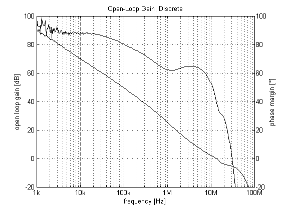
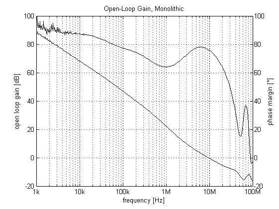
As can be seen, the discrete implementation has both a slightly higher open-loop gain and considerably worse phase margin. In simulation, I didn't see the poor phase margin and the slight peaking at about 15 MHz. I suspect that the low-noise transistors used for Q5 and Q10, which I replaced with 3904/3906 in the simulation, are part of the game because they have relatively high junction capacitances. Possibly a poor layout (which was done in a hurry), contributed too.
Now the voltage and current noise measurements:
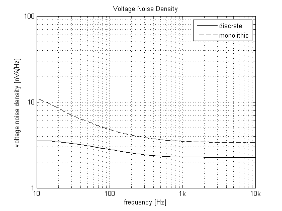
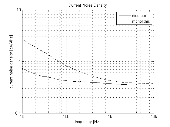
Here the discrete is a clear winner. That's most likely because of the low noise transistors I've used, and the absence of later PNPs (which have high current noise) for Q1.
Finally a few THD+N measurements (the first three done at 40 dB noise gain, then referred to the input by subtracting 40 dB):
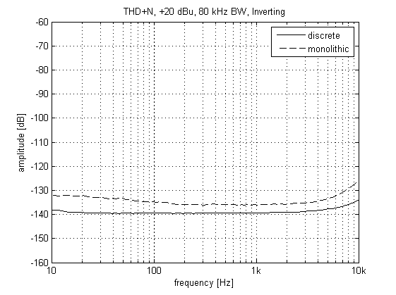
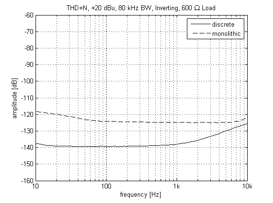
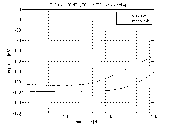
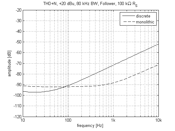
Mostly because of the improved output stage (and probably also because of the absence of thermal effects and higher output impedance of the input stage current source), the discrete version wins in the first three cases; below 1 kHz, the measurement data is dominated by noise and the measurement system residual. In the case of high source impedances in noninverting configurations, the monolithic opamp shows lower distortion. I suspect that it uses transistors with small geometry for the input stage, which have lower collector-base juncation capacitance than the low-noise/large geometry parts I've used.
Samuel
The last prototype PCB run at work had a bit of space left, so I decided to implement a discrete version of the NE5534 there. I didn't had particular intentions, that's just for fun.
Here's the schematic: discrete_NE5534.pdf
It implements a few changes over the original monolithic circuit, in order to take advantage of the possibilites, and to circumvent the limitations, of a discrete implementation; in particular these are:
* Biasing is done by 1.24 V bandgap references; the gives proportional-to-absolute-temperature (PTAT) currents. This is advantageous as it keeps the transistor transconductances, and thus the basic open-loop gain and stability margins, independent of temperature. The original bias circuit requires emitter ratios, which is inconvenient to implement at the PCB level.
* The voltage reference of the current source which biases the input stage is low-pass filtered by R12/C7; this reduces the noise impact of the reference, which becomes non-negligible at high frequencies (above the audio band) as the CMRR of the input stage degrades.
* C2, which is part of the compensation scheme, is connected to ground rather than a supply rail. This improves PSRR at high frequencies.
* Q7B is connected to the positive rail rather than the collector of Q9A. IIRC this give slightly better stability margins.
* C4 shunts the output stage bias elements at high frequencies. This aids stability margins a bit as both output transistors now see the same low drive impedance at HF.
* The output stage is now a fully complementary emitter follower. The original NE5534 is implemented on an old process which has just slow later PNPs; it thus uses an output stage with rather asymetrical output impedance (much lower for sourcing currents than for sinking), which is a dominant distortion mechanism when driving significant loads.
Otherwise the circuit and bias conditions closely follow the original.
Let's see how the discrete compares with the monolithic version; the open-loop responses start:
As can be seen, the discrete implementation has both a slightly higher open-loop gain and considerably worse phase margin. In simulation, I didn't see the poor phase margin and the slight peaking at about 15 MHz. I suspect that the low-noise transistors used for Q5 and Q10, which I replaced with 3904/3906 in the simulation, are part of the game because they have relatively high junction capacitances. Possibly a poor layout (which was done in a hurry), contributed too.
Now the voltage and current noise measurements:
Here the discrete is a clear winner. That's most likely because of the low noise transistors I've used, and the absence of later PNPs (which have high current noise) for Q1.
Finally a few THD+N measurements (the first three done at 40 dB noise gain, then referred to the input by subtracting 40 dB):
Mostly because of the improved output stage (and probably also because of the absence of thermal effects and higher output impedance of the input stage current source), the discrete version wins in the first three cases; below 1 kHz, the measurement data is dominated by noise and the measurement system residual. In the case of high source impedances in noninverting configurations, the monolithic opamp shows lower distortion. I suspect that it uses transistors with small geometry for the input stage, which have lower collector-base juncation capacitance than the low-noise/large geometry parts I've used.
Samuel
