Leonardori
New member
- Joined
- Jul 28, 2016
- Messages
- 2
Hello, I want to post my project here .I hope you can correct me if there are mistakes. And I hope my experience can give you a little help .
Exposition time:
One could call me a freshman in electronics and I just designed my first little audio amplifier for headphones. (Pocket design, I want to be able to drive 4 headphone pairs from a single source) Here's the schematic, so you guys know what I'm talking about:
(Without power supply (9V bat) and single channel)
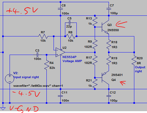
Ofc, 4 headphones draw a lot of current, which is why I need a proper output stage. Up to 200mA to be precise. The current design I made uses 2N5551 and 2N5401 transistors but their DC current gain is horrible (<10) which causes the OPA to overdrive. I don't want to much load on the OPA as well (max 20mA). A higher input voltage is out of question.
Therefor I need better output transistors (Q3 & Q4) which provide a higher current gain but also are capable of switching fast enough for audio signals. They should be cheap and small. I don't know that much components and the market out there is just a jungle of different parts.
The question:
Is it possible to compensate for the clipping with different output transistors? The circuit behaves great on 32 ohm but a lower load impedance wrecks it. I'm also open for darlington array solutions.
*EDIT: I can't use SMD parts. I need through hole packages.
**EDIT: Juuuust figured! This OPA is not even able to supply 20mA, because R9 & R17 are to large. In that case, a darlington setup with the current transistors could work, I just have to lower those resistors. Will keep you guys updated.
________________________________________
Solution: There's more than one solution to this problem:
1. Use a different OP amp which can drive the transistors rail to rail (see accepted answer). This only works if the 2N5551 and 2N5401 output transistors are configured in a darlington setup. However, the OPA used in this circuit almost drives rail to rail, already. (+-4V on the output)
2. Other output transistors with a better gain. 8550 (PNP) and 8050 (NPN) behave greatly for this application, they still need a darlington setup, though. (Special thanks to Spehro Pefhany)
3. Increase the supply voltage. This works like a treat, IF you're actually able to do so. Sadly, I am not in my setup.
4. Replace the output stage with a "diamond buffer circuit". It performs well in the simulation, did not test it on the bread board, yet. But it's nature of a voltage follower driving the push/pull transistors decreases the total swing of the op-amp, which results in better slew rates and therefor also frequency response of the circuit. Thanks to ioplex for adding this in.
My Solution:
I kept the OPA and used a darlington setup on the output. On my previous tests I forgot to modify the voltage divider to adjust the offset voltage between both transistors. I fixed that and now the circuit works. No clipping even on the worst input signals, that's what I wanted. Tests with my bench supply show that it actually operates down to +-3V which is great if you consider the voltage drop on the battery as it decharges over time. This is just the first design, I will change some things in the future. It is pretty clear that this is not the best setup and that I'm not using the best components for it. Design goals, however, were low component costs and supply voltage. And these are met with a decent performance of the circuit. It does sound gorgeous, feel free to try it yourself!
Thanks to everyone for the help I learned a lot through this project.
Here is the new schematic (2N5550 is a 2N5551):All the components were from :http://www.kynix.com/
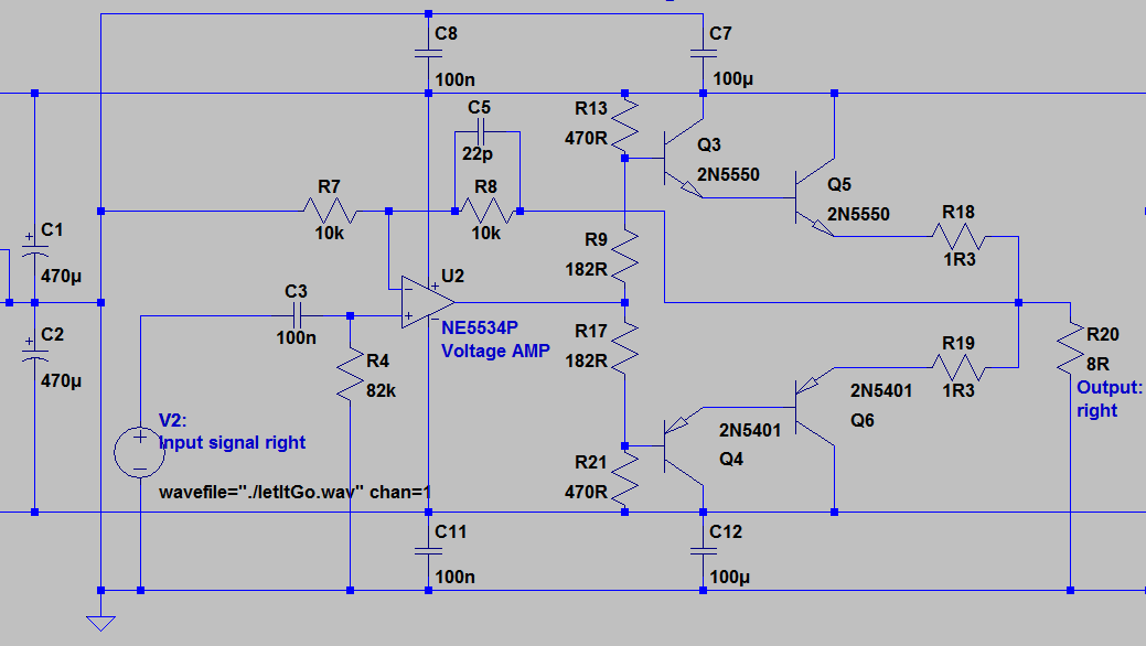
PS: What's no in this schematic is the compensation cap on the COMP - COMP/BAL pins of this particular op-amp. It's 47pF but LT-Spice has no proper symbol for the NE5534P.
Exposition time:
One could call me a freshman in electronics and I just designed my first little audio amplifier for headphones. (Pocket design, I want to be able to drive 4 headphone pairs from a single source) Here's the schematic, so you guys know what I'm talking about:
(Without power supply (9V bat) and single channel)

Ofc, 4 headphones draw a lot of current, which is why I need a proper output stage. Up to 200mA to be precise. The current design I made uses 2N5551 and 2N5401 transistors but their DC current gain is horrible (<10) which causes the OPA to overdrive. I don't want to much load on the OPA as well (max 20mA). A higher input voltage is out of question.
Therefor I need better output transistors (Q3 & Q4) which provide a higher current gain but also are capable of switching fast enough for audio signals. They should be cheap and small. I don't know that much components and the market out there is just a jungle of different parts.
The question:
Is it possible to compensate for the clipping with different output transistors? The circuit behaves great on 32 ohm but a lower load impedance wrecks it. I'm also open for darlington array solutions.
*EDIT: I can't use SMD parts. I need through hole packages.
**EDIT: Juuuust figured! This OPA is not even able to supply 20mA, because R9 & R17 are to large. In that case, a darlington setup with the current transistors could work, I just have to lower those resistors. Will keep you guys updated.
________________________________________
Solution: There's more than one solution to this problem:
1. Use a different OP amp which can drive the transistors rail to rail (see accepted answer). This only works if the 2N5551 and 2N5401 output transistors are configured in a darlington setup. However, the OPA used in this circuit almost drives rail to rail, already. (+-4V on the output)
2. Other output transistors with a better gain. 8550 (PNP) and 8050 (NPN) behave greatly for this application, they still need a darlington setup, though. (Special thanks to Spehro Pefhany)
3. Increase the supply voltage. This works like a treat, IF you're actually able to do so. Sadly, I am not in my setup.
4. Replace the output stage with a "diamond buffer circuit". It performs well in the simulation, did not test it on the bread board, yet. But it's nature of a voltage follower driving the push/pull transistors decreases the total swing of the op-amp, which results in better slew rates and therefor also frequency response of the circuit. Thanks to ioplex for adding this in.
My Solution:
I kept the OPA and used a darlington setup on the output. On my previous tests I forgot to modify the voltage divider to adjust the offset voltage between both transistors. I fixed that and now the circuit works. No clipping even on the worst input signals, that's what I wanted. Tests with my bench supply show that it actually operates down to +-3V which is great if you consider the voltage drop on the battery as it decharges over time. This is just the first design, I will change some things in the future. It is pretty clear that this is not the best setup and that I'm not using the best components for it. Design goals, however, were low component costs and supply voltage. And these are met with a decent performance of the circuit. It does sound gorgeous, feel free to try it yourself!
Thanks to everyone for the help I learned a lot through this project.
Here is the new schematic (2N5550 is a 2N5551):All the components were from :http://www.kynix.com/

PS: What's no in this schematic is the compensation cap on the COMP - COMP/BAL pins of this particular op-amp. It's 47pF but LT-Spice has no proper symbol for the NE5534P.


