


Skylar
Well-known member
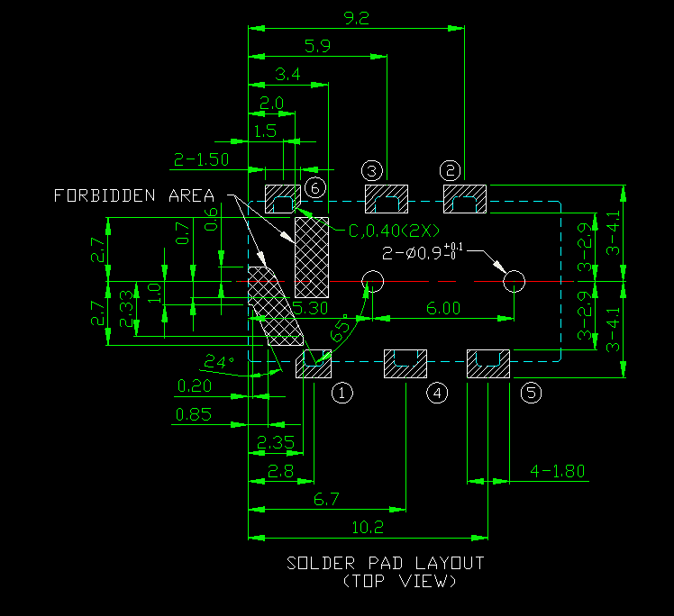
I'm having a discussion with a colleague concerning a component footprint drawing...a 3.5mm jack.
He says the areas marked "Forbidden Area" are intended to be PCB pads.
uhhhhhh, I don't think so!
Someone back me up. Or am I missing something?
He says the areas marked "Forbidden Area" are intended to be PCB pads.
uhhhhhh, I don't think so!
Someone back me up. Or am I missing something?