I was reading something on the web about the Urei 1176 "slam" mode where all 4 compression ratio buttons are pressed together. The author seems to conclude that the slam mode is largely equivalent to a 10:1 compression ratio. I was just modelling the Urei 1176 compressor in LTSpice and what I see is quite different.
The "slam" mode short-circuits 3 of the 5 resistors in the resistor network of the switch. This causes much more current to be drawn through it. So instead of 1.62 mA, it's drawing 2.98 mA. Because this is connected directly to the bias voltage divider, it *pulls the bias down* significantly. The quiescent point of the control votage (CV) goes from -2.0 V (at least in my model, this is adjustable using the trimpot) to -3.2 V. Because more rectified signal is require to overcome this difference, the attack becomes longer but the CV reaches higher.
This is the CV in reaction to a 1 kHz burst:
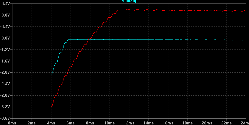
Red is slam and blue is normal. You can see the control voltage of the slam mode is quite different.
This is the resulting attenuated signal at the drain of the JFET:
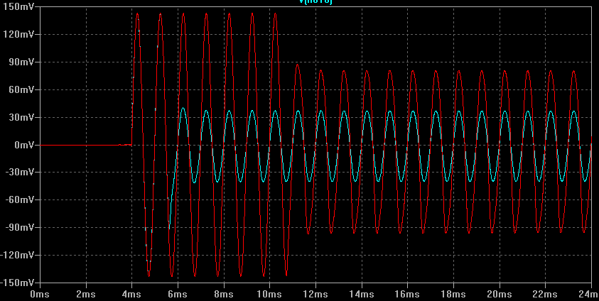
Again the red trace is with all-buttons-in and blue is without. Notice that the "slam"ed signal is actually attenuated *less*.
And here is the JFET gate:
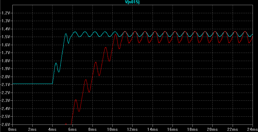
This is perhaps the most interesting. The JFET gate is supposed to get exactly 1/2 of the input signal so as to cancel distortion. But it appears this anti-distortion signal is distorted itself by the extra load on the DC point of the CV.
So in crude terms the control voltage is being distorted by the extra load on the bias. It would not be a leap to compare this to "sag" in a guitar amp.
The "slam" mode short-circuits 3 of the 5 resistors in the resistor network of the switch. This causes much more current to be drawn through it. So instead of 1.62 mA, it's drawing 2.98 mA. Because this is connected directly to the bias voltage divider, it *pulls the bias down* significantly. The quiescent point of the control votage (CV) goes from -2.0 V (at least in my model, this is adjustable using the trimpot) to -3.2 V. Because more rectified signal is require to overcome this difference, the attack becomes longer but the CV reaches higher.
This is the CV in reaction to a 1 kHz burst:

Red is slam and blue is normal. You can see the control voltage of the slam mode is quite different.
This is the resulting attenuated signal at the drain of the JFET:

Again the red trace is with all-buttons-in and blue is without. Notice that the "slam"ed signal is actually attenuated *less*.
And here is the JFET gate:

This is perhaps the most interesting. The JFET gate is supposed to get exactly 1/2 of the input signal so as to cancel distortion. But it appears this anti-distortion signal is distorted itself by the extra load on the DC point of the CV.
So in crude terms the control voltage is being distorted by the extra load on the bias. It would not be a leap to compare this to "sag" in a guitar amp.


