boji
Well-known member
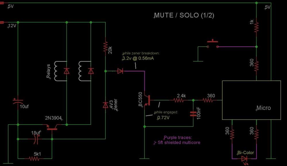
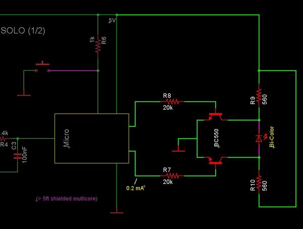
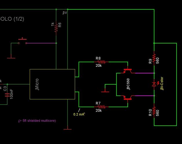
When using a two pin bi-color led, is there any standard shift register technique for swapping anode/cathode pins? Going to guess the solution would be to double-up on them so to get a source/sink (red), sink/source (green) or sink/sink (off) state delivery to two pins.
Perhaps there's a better ic to use, one where pin output states are flexible and can drive a bunch of leds?
So far the only thing I'd be confident coding-up would be a few atmel megas, banging out pinstates 1:1, sent to buffers.
Perhaps there's a better ic to use, one where pin output states are flexible and can drive a bunch of leds?
So far the only thing I'd be confident coding-up would be a few atmel megas, banging out pinstates 1:1, sent to buffers.
") Should have waited to speak up.
Should have waited to speak up.