boji
Well-known member
Vbe(on) minimum 580mV? Am I reading that right?
Obviously it's taking much less to switch on.
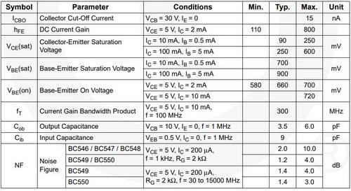
Obviously it's taking much less to switch on.


Well, I've not settled on a led yet. Still believing some may require standard 20mA. But wow yeah, these particular ones are efficient. Mega has about 60 available pins,At 5ma you don't need the transistors. And I don't see how you're going to do 55 leds with one micro.
Now that shift registers have arrived going to try to incorporate some hex inverters to see if I can minimize pincount as you suggest, I'm just not that strong at writing code for IC's. Perhaps the inverters will provide the buffering for leds as well, so to omit the transistors.maybe just an I/O expander
it's not clear how that would work with bi-color LEDs.
boji said:Duh. What would I do without you guys eyes-n-brains...Thank you!
I ASSume because they leave the minimum blank, any microcurrent value that will get the leg to show proper voltage will do the do.
yessr. thanksShielded CAT6 could probably make it a meter or so with the right clock speed and termination resistors.
void chipselect(uint8_t i) {
  if (i > 7) return;

  Wire.beginTransmission(PCA_ADDR_1);  //1 of 8 I2C bus addresses
  Wire.write(1 << i);                  //1 of 8 Pin expander chips on given I2C bus
  Wire.endTransmission();
}chipselect(1); // prep to test leds I/O expander 1
for(int i = 0; i <=15; i++) {
mcp1.digitalWrite(i, HIGH);
delay(200);
mcp1.digitalWrite(i, LOW);
delay(200);
}
chipselect(2);//switch and prep
for(int i = 0; i <=15; i++) {
mcp2.digitalWrite(i, HIGH);
delay(200);
mcp2.digitalWrite(i, LOW);
delay(200);
}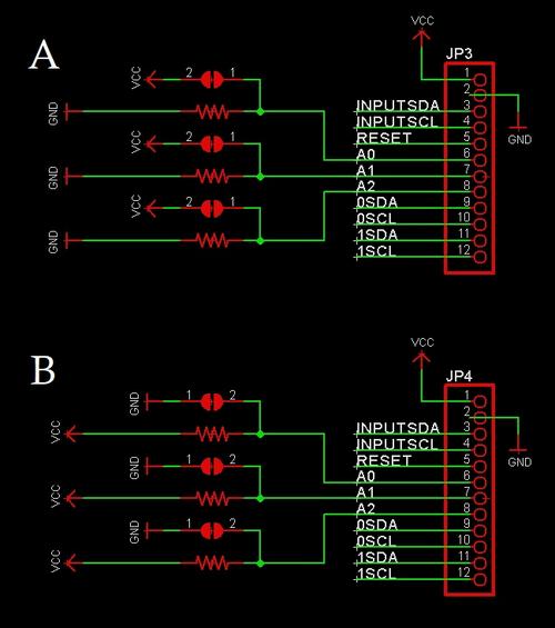
I vote for B, since I don't like having Vcc (or Vdd) distributed to too many places without protection.boji said:Happy Holidays everyone. I've seen address assignment of I2C chips done both ways as shown below. Do you have a preference and if so, why?
Not necessarily.Note for B, resistors are left out or included so to define assignment, whereas for A, resistors are included no matter the HEX value.
Think I understand, because Vcc could be 3.3 or perhaps lower in some scenarios.Not necessarily.
Yeah I struggled with this decision but perhaps concerns are unfounded. Figured a bundle of shielded i/o wires are better than having a 'digital' pcb in each bucket (right under unbalanced fader lines) chunking away 24/7. I agree it would be much simpler to put extenders near the i/o endpoints. Looking for a slimline case to shield pcb's, but finishing is becoming more important than anything at this point. :/you're going to have potentially long control cables?
5v and Gnd planes included, quite objectively to drain those transistors and pull up button sensing i/oOr, if you do it the way you have it layed out, what is the ground plane situation?
")
Yessr. Pulldown/debouncing circuits for relays are onboard each channel card that supplies 12v, and sinks most of it. I believe as long as m/c pcb's are tied to console dcom, max draw is 0.6mA @ ~3v per relay cv pin.might be desirable to have a decent ground plane below (or above) those lines to the transistors with a really good ground wire to DGND running right next to (or loosely twisted around) the relay supply wire.
Enter your email address to join: