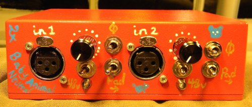
midwayfair
Well-known member
Here's the schematic (PDF): http://www.jlmaudio.com/BAN/BAN%20Schematic.pdf
I'm struggling to understand *exactly* how this works.
The part that's easy enough to figure out:
1) When the collector gains increase, they send more signal into the inverting inputs.
2) The non-inverting inputs of the op amp provide the collector voltage. Presumably because the specified transistor can't take 48V?
What I don't get:
3) How does decreasing the resistance between two emitters that are referenced to the output pins of the op amps increase the gain? My best guess is that the resistance between the base and collector drops while the resistance between the collector and emitter goes up, which would simply increase the gain of the non-inverting op amp stage, but I can't figure out how the gain pot accomplishes this simply by connecting the emitters together.
And misc. questions:
4) The gain pot crackles. Presumably this is unavoidable because a DC change is required to make the transistors behave this way?
5) I did notice that both test points 2 (gain pot "balance) and 3 (Vb) change depending on the gain pot's setting. I ended up balancing them with the gain at 0, which I assume is the only reasonable way to do that.
6) The few R of the gain range is unusably noisy (anything so quiet as to require that much gain would be drowned out by the hiss), though it's amazingly quiet up to the last of the turn (a good 6dB less than my interface's pres at approximately the same gain). I'm assuming there's no difference between changing the two emitter 10R to something between 15R--47R and limiting the gain pot position? I'm not sure exactly how to pick the value, though, without fully understanding the gain pot.


