[BUILD] CAPI VP312DI~500/51x Series~Preamp + Direct Inject~Official Support Thread

GroupDIY Audio Forum

Help Support GroupDIY Audio Forum:

This site may earn a commission from merchant affiliate links, including eBay, Amazon, and others.
I just added a new FET HiZ Plug-In module to the store for use in the VP312DI preamp. It replaces the old FET1.

Details are on the product page here http://capi-gear.com/catalog/product_info.php?products_id=571
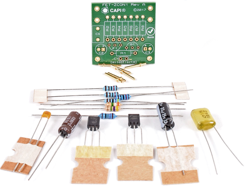
FET-ZCON1-parts.jpg
 
Hi guys, I love these kits and am about to start on my second 312DI. In a way, it seems like these builds go from pretty easy to hard and then pretty easy again.
I'm talking about hitting snags and troubleshooting. My first project was a VP26 and it went great until I somehow misaligned it when inserting it into a 51x 511 rack and the power resistor next to the OT caught fire when I powered up, oops!

Anyway, that's for another thread. My first 312DI build went great and seemed to work just fine initially but now when I switch on phantom power I hear a hissing and crackling, static like sound that comes and goes. Dynamic mics and the DI (IC) work fine. I reflowed the pushbutton switches but no improvement as yet. It does point to a cold solder joint somewhere just looking for suggestions where to start looking. Another symptom: when I push the pad switch, there is slight static and a pop, possibly DC leakage somewhere?

The rack is verified good as is the slot. Measuring 48V where it should be on the PCB.

I guess you could say I'm on a DIY uphill slope right now with: a VP26 with fried power resistor; a VP312DI with phantom power noise; a VP28 with a wonky output fader; a GAR1073 missing an 18K resistor; a GAR2520 where Q3 snapped off when I tried to nudge it to install Q2.

Waiting for a desoldering station and replacement parts from mouser to arrive to undo, undo haha. Good time for deep breathing...

 
pkordel said:
...My first 312DI build went great and seemed to work just fine initially but now when I switch on phantom power I hear a hissing and crackling, static like sound that comes and goes. Dynamic mics and the DI (IC) work fine. I reflowed the pushbutton switches but no improvement as yet. It does point to a cold solder joint somewhere just looking for suggestions where to start looking.
I do publish the schematic for this build. If you take a quick look you will see less than a handful of components involved in the phantom power circuit. I would look for a cold solder joint on one of those parts firstly the 120µF cap.

Another symptom: when I push the pad switch, there is slight static and a pop, possibly DC leakage somewhere?
The polarity switch is disrupting the signal between the opamp and transformer so it will never be 100% silent. It will indeed "pop" more if DC is present. I do recommend that you set the shunt jumper to "DC Block/Cap Coupled Output" especially if you ever use the pre in Post 2622 mode. If you want to verify the amount of DCV present, just probe between ground and one end of the 1Ω R. Again, use the schematic to locate the position. It won't be "DC leakage somewhere" it be DC getting to the polarity switch.
 
jsteiger said:
I do publish the schematic for this build. If you take a quick look you will see less than a handful of components involved in the phantom power circuit. I would look for a cold solder joint on one of those parts firstly the 120µF cap.
The polarity switch is disrupting the signal between the opamp and transformer so it will never be 100% silent. It will indeed "pop" more if DC is present. I do recommend that you set the shunt jumper to "DC Block/Cap Coupled Output" especially if you ever use the pre in Post 2622 mode. If you want to verify the amount of DCV present, just probe between ground and one end of the 1Ω R. Again, use the schematic to locate the position. It won't be "DC leakage somewhere" it be DC getting to the polarity switch.

Thanks Jeff, I'll try your suggestions later today. I do have the shunt jumper set to DC Block.

Cheers
 
I've been looking at the schemo for about the past two months now studying every part before working up the nerve to order/do this build....

How does VC of the PK1 relay connect to GND via BB3? Looks like that goes to the ring of the TRS jack when the Post 2622 switch is flipped,  but on the jack diagram itself, I don't see the ring connected to GND?  What am I missing here?
 
seanweaverguitar said:
I've been looking at the schemo for about the past two months now studying every part before working up the nerve to order/do this build....

How does VC of the PK1 relay connect to GND via BB3? Looks like that goes to the ring of the TRS jack when the Post 2622 switch is flipped,  but on the jack diagram itself, I don't see the ring connected to GND?  What am I missing here?
The function will only work when a mono 1/4 plug is inserted into the stereo jack. The jack is connecting ring to sleeve thru the plug itself.
 
jsteiger said:
The function will only work when a mono 1/4 plug is inserted into the stereo jack. The jack is connecting ring to sleeve thru the plug itself.

Ah yes, I'm slow checking back in here but that makes perfect sense now. Thank you very much for taking the time. I'm finishing up a blues guitar project and allotting funds for more projects once I get paid so I think a 312DI is in my future once I'm certain I'm not going to screw it up or at least have a full enough understanding to know how to troubleshoot the circuit if I run into problems (the Hairball builds were successful last winter but they were my first and I wanna make sure I really understand the schematics, have read through entire build threads, have the right equipment (got the Hekko, no desoldering station though; Fluke 179, but no oscilloscope or high powered magnification yet)  and am fully prepared to take on a project like this without a build rescue service....I think I'm close).

At this point the only thing still making me scratch my head is the -10dB pad in post 2622 mode. I'm probably reading the schematic wrong but working on it. Still not seeing how the pad circuit is completed with SW2 in either position. Really trying for weeks on end too.  Looks like in either position it's going through R1 & C2 on the Sub DI board but I'm not sure how or where it completes depending on which way the switch is flipped. If it's still not making sense in a couple more weeks I'll give up and post back here again.

(I'm doing the work, I'm baby-stepping. I really am hungry to learn this stuff)

Thanks for the clarification Jeff. I really do appreciate it
 
Hey guys,

I’m building  this mic pre, and I’ve ran into a problem, and there doesn’t seem to be a resolution through out the thread. Upon placing the sub DI 1 and placing it as described in the thread, on top of the main PCB, the switches for post 2622, -10, and J lpf, do not line up with the holes on the face plate. What it seems like is the sub DI PCB, looks like it should be on the bottom of the main PCB. Would this correct this issue?  I have already soldered the 5 leads to hold the sub DI PCB in place on top of the main PCB. So that makes it very hard to remove. But wanted to check here to see if anyone has had this issue? Attached is a picture of what it looks like with the face plate. Thank you.
 

Attachments

  • F5B1F4BA-6916-44F3-8F3D-4C149933153B.jpeg
    F5B1F4BA-6916-44F3-8F3D-4C149933153B.jpeg
    1.5 MB
Jroq82 said:
Hey guys,

I’m building  this mic pre, and I’ve ran into a problem, and there doesn’t seem to be a resolution through out the thread. Upon placing the sub DI 1 and placing it as described in the thread, on top of the main PCB, the switches for post 2622, -10, and J lpf, do not line up with the holes on the face plate. What it seems like is the sub DI PCB, looks like it should be on the bottom of the main PCB. Would this correct this issue?  I have already soldered the 5 leads to hold the sub DI PCB in place on top of the main PCB. So that makes it very hard to remove. But wanted to check here to see if anyone has had this issue? Attached is a picture of what it looks like with the face plate. Thank you.
I am guessing that you soldered the NKK switches onto the top of the PCB when they should be on the bottom? Please see step #4 on the very first post of this thread.
 
Hi Jeff,
As always thank you for your quick response.  I have in fact soldered them to the bottom,  As step 4 indicates. All the other knobs and push buttons fit nicely. Please See photo attached, to confirm switches are in correct. Hopefully you see something incorrect. Thank you.
 

Attachments

  • C6C88687-4730-43D5-8378-364928776F7E.jpeg
    C6C88687-4730-43D5-8378-364928776F7E.jpeg
    471.6 KB
Jroq82 said:
Hi Jeff,
As always thank you for your quick response.  I have in fact soldered them to the bottom,  As step 4 indicates. All the other knobs and push buttons fit nicely. Please See photo attached, to confirm switches are in correct. Hopefully you see something incorrect. Thank you.
Ah, OK now I see it. The t-pad was incorrectly soldered directly to the PCB which is throwing off the entire module's alignment.
 
jsteiger said:
Ah, OK now I see it. The t-pad was incorrectly soldered directly to the PCB which is throwing off the entire module's alignment.

So should I space it like it says for revision B, even though I have revision D? That would make sense, as it is slightly off.
 
Jroq82 said:
So should I space it like it says for revision B, even though I have revision D? That would make sense, as it is slightly off.
No, the steps for that start with #2 in the first post of this thread. The steps are fairly detailed out.
 
Alright I figured out the schematic (the DI pad part that was the last part I wasn't yet able to make sense of a few days earlier when I last posted). As funds come in I'll have one of these on my to-do list for sure. Still a little nervous to take on a project without a build rescue service not yet having an oscilloscope or other test equipment past the Fluke 179 (one step at a time) after a couple Hairball builds (both of which were successful) but think I can do this and very much look forward to before long. Thanks again for answering my question about how the PK1 relay connects to GND through the ring. That really helped and now I more or less understand the schematic. I'm on a mission to keep learning and build more gear in the process & this is one high on my list so you'll definitely be hearing from me. Thanks again Jeff 
 
I just finished building my second VP312. Everything seems to be working fine, except phantom power is not powering up, or LED is lighting up.
I doubled checked and went through possible, suspicious soldering spots, but doesn't seem like helping.
What would be the instant places I should be checking for this issue? Any help would be greatly appreciated!
 

Attachments

  • IMG_1475.jpg
    IMG_1475.jpg
    1.6 MB
shogami said:
I just finished building my second VP312. Everything seems to be working fine, except phantom power is not powering up, or LED is lighting up.
I doubled checked and went through possible, suspicious soldering spots, but doesn't seem like helping.
What would be the instant places I should be checking for this issue? Any help would be greatly appreciated!
Its hard to tell in the pic but it appears that the LED leads are shorted against each other? Might be an optical illusion. The schematic is published for this build so you can see where to measure for 48V if you check the skiz.
 
jsteiger said:
Its hard to tell in the pic but it appears that the LED leads are shorted against each other? Might be an optical illusion. The schematic is published for this build so you can see where to measure for 48V if you check the skiz.

Hi Jeff,

Thank for your guidance. I've checked out the schematics, tested out the unit for few days.
Did some continuity test with DMM, especially around BB1, BB8 and BB4 pin, seems to be making a healthy connections. LED wasn't shorted.
There was a healthy continuity from J2-15 to SW6.
At this point I'm not really sure what is causing phantom to not work...LED is still not turning on, nor the 48V.  :'(
Everything else functions perfectly,  from all the mute, phase etc, to DI functions.

Uploaded few more photos...

https://www.dropbox.com/sh/zcn80x714q87roh/AACcsugg293kMOAxLvbU8XG3a?dl=0

Sorry for taking your time, but again, any help will be greatly appreciated!

Sho
 
First of all.
Which kind of lunchbox do you use ? I had some trouble with a Bento2 with the phantom power. The power board had some problems and the regulator fired up two times.

Second:
You had some solder joints who look really bad.
You should definitely resolder some points (there are lot of joints where you can see the gold solder pads)
95% of problems are poor solder joints.
Also use some isopropyl to clean the pcb.
 

Latest posts

Back
Top