CAPI-Gear; CA-0252 (2520 Type), CA202 Opamp Kits and DIY Parts Galore!!!

GroupDIY Audio Forum

Help Support GroupDIY Audio Forum:

This site may earn a commission from merchant affiliate links, including eBay, Amazon, and others.
jsteiger said:
A couple of modules I have are TH with PTH's. Without desoldering something on them, I am not sure how oversized their component holes are. There is definitely a good complete joint on each side. How it was done is an educated guess. My educated guess is that they are pumping out as much product as they can which absolutely correlates to "you better only solder one side or you are fired"!! Time is money of course.

I would be surprised if any medium-to-large scale TH production in the last decade has been done by hand, given that wave soldering technology is relatively inexpensive and very mature. Maybe some smaller players in the Mainland or the Philippines still hand solder, but I doubt it.

jsteiger said:
Anyhow, knowing that the big production assembly houses aren't doing it...is probably a good enough reason to do it!

The ones I've been involved with are mostly smaller specialist shops doing Hi-Rel proto and short-run work for industrial and military/aerospace projects. ICBW, but they've never given me the impression of rushing their staff, given that at the end of the day reliability and yield targets have to be met. (As with software bugs, it takes much longer to find and fix a marginal joint than to get it right the first time)

A few years back I was asked to hold a few EE-centric workshops for design students. As you might imagine, most had little to no soldering experience. Watching them work I got the strong impression that novice solderers are more likely to heat joints for too long. As too much heat can easily damage components and boards (through delamination), I would be hesitant to suggest any technique that encourages people to heat the joints even more. Soldering from the top has the added disadvantage of having the heat source closer to the component body, which can be especially bad for diodes and the like.

(I did notice that you only suggest to touch up after snipping the leads, and your staggered soldering procedure for the switches looks like a good idea. At the end of the day it's your guide, your decisions, and I'm not the one who gets to deal with board failures or returns. Your call.)

JDB.

[EDIT: grammar]
 
Hi guys,

I am currently sold out on Ed's 2622's but have another 100pc batch due end by the end of next week.

I am also working on another cool 51x compatible project that I should have the proto board for in about a week or so. Options are good right?  8) There will be a few pretty cool special announcements involving this new board coming over the next few weeks. Also a few unique variations coming too.

I have a couple of new C&K switches that will be added to the store over the next few weeks. A little arm twisting from Matta can go a long way!  ;)

Oh, I have also pestered Gary long enough about another DOA that is pin compatible with the 2520. We are in the testing and listening stages now. If all pans out and we are happy with the results, we will carry PCB's and parts kits for this one just as we are with the gar2520. Will keep you posted with this as it develops.  ;D

Cheers, Jeff
 
gar381 said:
...Jeff should be fully stocked with
gar2520 PCBs and kits by mid week.
Thanks for the prompt service as always Gary! 8)

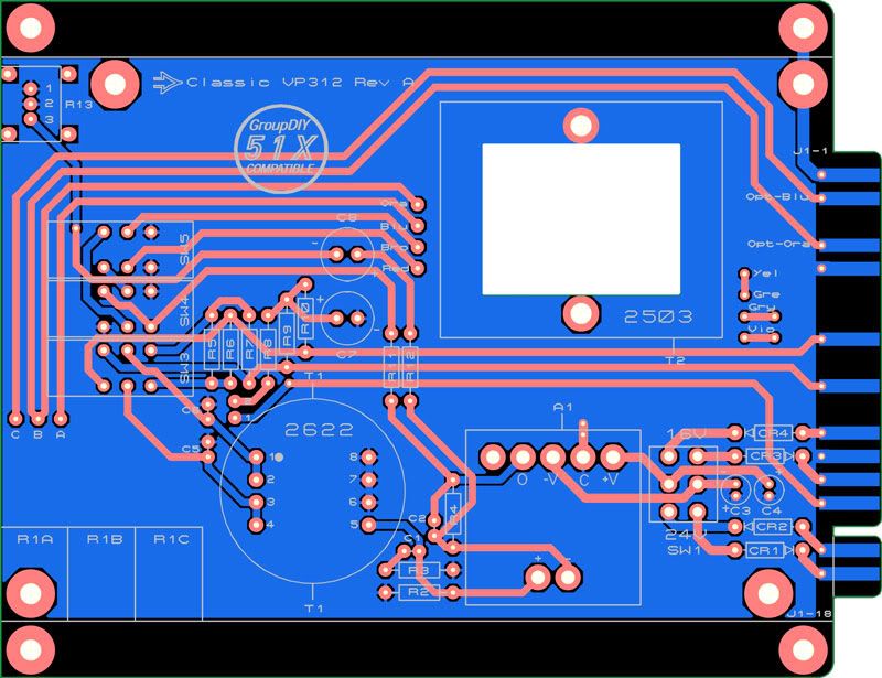
I've got a fun little project going that I posted last night on the rack thread. It's a simple, straight up 312 circuit 51x style....with a few twists. I've made the voltage rails to the DOA switchable for a Forsell, JLM, Hardy or whatever. The extra pins can easily be snipped off ala Peter Purpose if someone will only use it in a standard 500 rack. The full board as is mounts to my current L-bracket and the faceplate layout is identical as my VP2x stuff. That board width is 4-1/2", standard 500 size. As you can see, I have 2 horizontal lines in the silk where the copper pour stops. There are also 4 additional inner mounting holes. By trimming the board along both of these lines, you remove 3/4" in total, leaving you a PCB of 3-3/4". So, 4 of these will easily fit in a 1U rack, side by side, for someone who is anti 51x or 500 series all together. That I can't figure out but to each his own!

I have a proto ordered. Should get here by next Monday. These boards will be in a sexy matted black.  ;)

Here's a screen shot...
VP312-PCB-SS.jpg


Cheers, Jeff
 
Hey guys,

I have received some more gar2520 boards and kits as well as EA2622's. Store stock has been updated.  ;)

Cheers, Jeff
 
matta said:
Any word on the VP312 proto? It looks DARN sexy by the way  8)

Matt
Thanks Matt! Sexy is good.  :)

Looks like it is due here on the 28th, which is next Thursday. The board house had a couple of questions on the file. The offset solder pads for the gain pot always throw them. That and they asked if I wanted the 2 horizontal silk lines v-scored. I told them no v-score. So, their lead time starts ticking once I confirmed that the files were correct. I like how they are so careful.  ;D

Funny thing, I ordered the proto and upload my files to them before I posted the screen shots here. Once I posted the screen shots, I noticed a double "T1" label in the silk layer!!  ::) So, I'm glad they had the questions as it gave me a chance to update the silk layer!!

I will keep you posted.

Cheers, Jeff
 
I have just uploaded an updated version of the VP2x Assembly Guide for those who care. I had a small typo to fix thanks to Dan from Dan's Front Panels for spotting it "Jeff, it should be quiet switching, not quite switching"! Duh.

Also, per some razzing from JDBaker, I have modified my "solder from the top first" suggestion a little. The paragraph from the Assembly tips and pointers now reads like this:

When possible, depending on the component you are soldering, try working from the top or
silk screen side of the PCB. After completing the required solder joints, flip your PCB over,
carefully clip the component leads and touch up the solder joint to the bottom solder pad if
needed. It should be noted that this bottom touch up is not a required step especially if a good
joint is made while soldering the top. I myself like this as it makes for a really nice and solid
construction. Special care must be taken to not apply too much heat as components can easily
be damaged. Excessive heat from the soldering iron or desoldering tool can lift and/or damage
the solder pads or traces of the PCB too so…BE CAREFUL!!!


I understand JDBaker that I am the one dealing with the returns and problems. So far, knock wood (my head in this case), over 250 boards out in the world and zero returns due to board failure. Heck, zero returns period. I only hope that continues. Thanks all.

Cheers, Jeff
 
Well my proto VP312 board has been shipped and will be here next Monday. I plan on building and testing right away so I can get some stock ordered to carry at the store. Funny how an 8 day turnaround suddenly turns into 15 days.  ??? It's the first tough experience I have had with my board house so I really shouldn't complain to much.

I have also completed layouts for my new series of faceplates. I have 200 raw faceplates due in on Monday as well. I plan on getting 50pc screened for the VP25, 50pc for the VP26 and 50pc for the new VP312. If I get the chance, I will post some artwork this weekend. They look pretty cool, IMHO.


Cheers, Jeff
 
[silent:arts] said:
Jeff, I'm modifying some "plug-in" PCBs right now to have them made by Lukas ;)
will send you some, will be a lot of fun ;D
"Plug-in" PCB's??? What the heck are you talking about Volker???  :-X
 
The sky is falling . . .  Headz up that your site's down, guess I'll go buy some head cheese instead
 
bdubya said:
The sky is falling . . .  Headz up that your site's down, guess I'll go buy some head cheese instead
I just check and all looks good from here. You had no access at all?
 
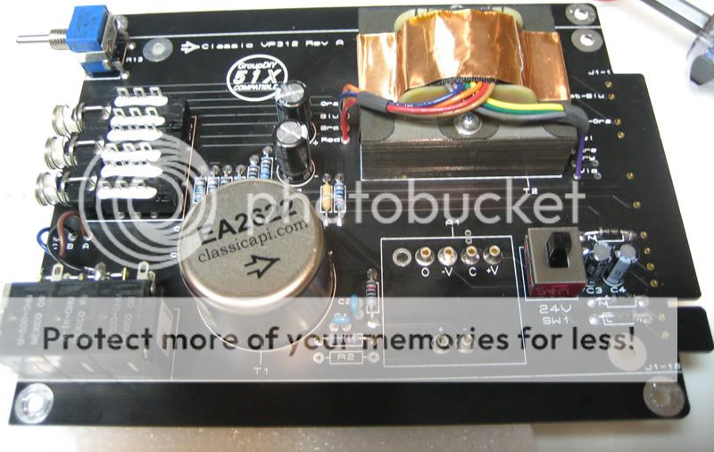
My VP312 proto board is here! 99% stuffed and ready to test. She looks super sweet in person!

I have to rig an edge connector for testing as I don't have access to a 51x rack yet... ???

R2 is the load R which seems to be a little controversial so, if you want to use it fine. If not that's fine too.

Anyhow, here's a quick shot. More tomorrow.

VP312-proto.jpg


Cheers, Jeff
 
Jeff, looks great! I love the white silk on black pcb.

What is it about the load resistor? Are you talking about the input TX secondary load?

Cheers

Mike
 
mikefatom said:
Jeff, looks great! I love the white silk on black pcb.

What is it about the load resistor? Are you talking about the input TX secondary load?

Cheers

Mike
Thanks Mike. I really like the color combo as well. It really suites the legend of the 312 just right.

Yes on the load R. I have been using it on the VP25 and 25 cards with great success. There was some debate as to whether or not that load was included on the vintage 312 cards. It is not on the 312 schematics floating around but that doesn't really mean too much. And like Ed says, a 150K load R is small potatoes anyhow.

Cheers, Jeff
 
WHOA!

Jeff, that thing needs shades, it is just that cool! I'm thinking aviators and a jump suit ala TopGun? LOL. Kudos, looking great, the black and white look fantastic together. Look forward to reading your review of the proto and testing with a +24V opamp.

Cheers

Matt
 

Latest posts

Back
Top