DBX902 - Anyone know much about the DBX RMS module?

GroupDIY Audio Forum

Help Support GroupDIY Audio Forum:

This site may earn a commission from merchant affiliate links, including eBay, Amazon, and others.
Well that's very honest of you Wayne. We used 2 Dynaflangers on a Cure record to good effect many years ago. It was an interesting effects box but the sound was a little thin.
In the 80's I experimented with a Reticon chip sandwidged between 2 Telcom NR chips (remember the Telefunken NR system ?). It was quite impressive but not as dramatic as the DBX arrangement - especially when using feedback.
The Time Modulator has an additional limiter (Vactrol) to help with regenerative effects. I guess that Steve probably stockpiled a load of SAD1024's when he realised that they were going out of production. He used to refer to the delay chips as 'analogue RAM'.
It's interesting that they are re-creating a few of these units - I think they will be hard pressed to find 303 boards.
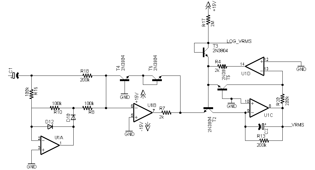
The possibility of creating a one-chip version of those DBX boards is what sparked my interest in the thread in the first place.
Martyn
 
As I said I won't argue opinions, especially about what people hear, but I do have some experience and a possible data point for you. I was working with BBD analog shift registers from Phillips in the early '70s before they licensed the technology to Matsushita (Panasonic MN series) and well before Recticon got into the game.

NR was mandatory for any kind of critical use since the channel S/N of BBDs was horrible at lower clock rates. My early work with BBDs predates the 570 compandor IC and I used a simple OTA (CA3080) pair to compress and then expand the audio signal to get a decent S/N.

I had this technology in products in several markets. My $39 kit flanger even found itself on one record, I know of (Heart's "Barracuda"). One product was a studio delay line/flanger with a decent local reputation in the northeastern US (LOFT 440/450). In a later design upgrade I went from 4x Recticon 1024s to a single 4096, and changed from 3080 NR to NE572. I did receive some feedback from studio users who preferred the old 440 "sound" to the newer 450. The longer Recticon delay chips is pretty similar in character, while perhaps a little cleaner in use than the shorter 1024 due to demands of multiple biasing.

The older design had more low order distortion from BBD bias errors, and the 3080 compander also added significant low order harmonic distortion. Some customers may have liked this extra distortion or I could have made some subtle changes in the regenerative feedback which is multiplied in use. Since I didn't use a limiter in the loop I had to run my max a little cooler than the Marshall. (The limiter is useful there because the BBD transfer function changes enough over the full range of clock frequencies that the optimal setting is compromised by the simultaneous requirement of stability at worst case).

Since I expect the dBX NR to be even lower distortion than NE57x series, which was already well below the BBD, the sound character will be even more defined by BBD nonlinearity and associated loops. I have never had any interest in knocking off the Marshall, but I would focus on regenerative feedback paths (frequency shaping, relative polarity, limiting, etc) , and perhaps DC biasing at clock extremes. BBDs are not very clean or well behaved devices. Use of a limiter in the feedback path allows running it at the hairy edge of instability for all clock frequencies which will give the most dramatic comb effects while flanging.

Have fun and good luck... The dbx chipsets are now cheap enough and available, but to play the devils advocate, the old dbx NR sets weren't as clean as the new stuff, so be careful you aren't missing some old distortion that inadvertently contributed to the overall effect. Assumptions are a good starting point, but test them and don't be over invested in a single theory.

My bet is the Marshall mojo is in the regenerative feedback path. and perhaps some extra grudge from DC bias shift, but you're entitled to a contrary opinion.

JR


PS: I really liked the Recticon CCD delay chip (R5101). I used it in one consumer (Bozak) hifi delay line and it worked quite well. But they obsoleted that part while I still had production running.
 
Wayne: Not to quibble but the RMS circuit seems to be missing a term. The math algorithm used to mimic RMS is "the square root of the integral of the signal squared". The circuit as shown drops the ball in the final square root function.

The diode connected FW recitifier logs the signal and use of two juntions in series (and gain of -2x in inverting amp) delivers the "square" function, with C17 "integrating" that squared term. The final Q4 could complete the square root function with another opamp or two and some specific current paths. There is also some pre-emphasis built into the rectifier, but that will just generate a frequency response error term.

I would classify this as a "quasi-RMS" circuit. It does share the attack characteristics of real RMS, but will look like true RMS at only the one level where the fixed output bias current equals the square root of the input. It will diverge from true RMS at higher and lower levels. This will under report at low levels and over report at high levels, which may be useful in some applications.

FWIW.

JR

PS: For best tracking, Q4 the square root device, should be one of the transistors from the array. The more popular approach is to do the rectification prior to logging, to accomplish this all within a single 5 transistor array.
 
From the that link:

"Taking the Square Root
The square root por tion of the Root-Mean Square
is im plied by the con stant of pro por tion al ity for
the out put volt age: it is not com puted ex plic itly.
This is be cause, in the log rep re sen ta tion, tak ing
the square root is equiv a lent to di vi sion by two.
The volt age at pin 6 is pro por tional to the mean of
the square at ap prox i mately 3 mV/dB, and pro por -
tional to the square root of the mean of the square
at ap prox i mately 6 mV/dB. " (sorry about the poor cut and past)
--------
They are performing the square root operation by scaling the log domain result. In log domain math, divide by 2 is equivalent to performing a square root operation. This is certainly accurate enough assuming all Vbe junctions track and are well behaved such as inside an IC.

This scaling of the output voltage in log domain was not apparent to me so I stand corrected. I still have concerns, but don't need to spiral off into esoteric trivia. For more general purpose RMS conversion where you need a well behaved linear output the square root operation must actually be performed and offsets well managed.

YMMV

JR
 
Not to be pedantic, but Q1 and Q6 are not taking the square root, but actually squaring the current. A change in input signal, converted to current, causes a voltage change in Q4 + Q5 or 2x Q3 that is two times the log of the current change for a single Vbe junction. This two times voltage change causes a squared current change when decoded by Q1 and Q6. This attack characteristic is one of the desirable features of RMS detection. Q7 is subtracting a nominal fixed Vb-e offset and the square root is only performed mathematically for "changes" in log output by scaling the log voltage a factor of 1/2.

How does this relate to sound? Yes RMS detection offers a different and to many preferable response for a given audio envelope. For all intents and purposes this is real RMS as will work fine as long as you manage Vbe offsets and only operate in the log domain.

JR

PS: I am not throwing stones at Blackmer.. he did important pioneering work and this finesse of the square root term is quite clever when operating predominantly within the log domain. :thumb: :thumb:
 
Believe it or not I don't really enjoy picking nits with other peoples designs or imprecise language. While there is more there to chew on, I instead have chosen to increase understanding.

Here is the only link I could find easily to a more complete RMS detector http://www.national.com/ms/LB/LB-25.pdf but this looks like it was drawn to confuse more than inform, so I bucked up and drew my own simple basic RMS detector.

Caveat: This is offered proforma (in other words there may be mistakes or omissions). The FW rectifier is very basic so this is not offered as a tweaked out design, just to demonstrate the basic principles. We have supported longer threads than this just on the subject of rectifiers. For example I show discrete transistors but typically used a 5-transistor array for matching and thermal tracking.

The next opamp stage wraps two Vb-es in the feedback loop to generate 2x LOGx to effectively square the signal.

When this doubled (squared) voltage is applied to emitter of T2 it decodes 2xLogX into the current squared. This current is integrated by C2.

As C2 integrates up, R20 and U1D pulls that integrated RMS current through T5 to perform the square root operation, completing the RMS algorithm calculation.

To be useful for any playing along at home (with VCAs and dB gain control math), I added another Vbe drop to establish a 0VU reference. Transistor T3 is excited by a constant current and when the AC input current equals that static DC current there will be 0Vdc at the node labeled LOG_VRMS. Signals will generate a log voltage on the order of -3.3mV per dB above or below 0VU reference (set by 2M resistor). Note above 0VU signals generate a negative voltage output, below 0VU a positive voltage. This point obviously needs to be buffered and another opamp could easily, scale, buffer, and invert if needed.


RMS.gif


To visualize how this circuit works, imagine an initial condition of say -100 VU audio input. All the transistor Vbes are at some small stable nominal voltage, except for T3 our zero reference, so it will have a full 0VU drop across it and be sitting a few hundred mV positive, reflecting the -100 VU.

Next we input a 0VU step function. Immediately T4 and T6 step up to full 0VU Vbe drops. T2 instantaneously draws the 0VU current squared as C2 charges up. As C2 charges the current in T5 increases, increasing the Vbe drop of T5, reducing the Vbe and current in T2. At final equilibrium all of the transistor Vbe are equal, resulting in 0V =0VU. at LOG output, and the actual RMS voltage at U1C opamp output.

I have used variations on circuits like this in meters and sundry applications. I am not convinced the true RMS is all that useful, but it isn't very hard to generate. Also with the circuit I drew up the time constants are very well defined (C2 and R13) and can be easily changed.

JR
 
[quote author="JohnRoberts"]I believe you're making an inappropriate logical leap to assume the NR was the magic in Steve's delay line. There are lots of not so subtle interactions especially when you involve regenerative feedback.

For now I will respectfully agree to disagree.

Good luck, and I hope you find the mojo you are searching for.

I have no desire to revisit BBDs while they were very good to me back in the '70s and 'early '80s. Then is then and now is now...

JR[/quote]

To my ears the best sounding BBD flanger was the Electro Harmonix Standard Electric Mistress - why, because it had no noise reduction and little filtering!!! John, have you seen the ADA Flanger circuit modified for SAD 1024 (from MN 3010) with additional clock buffering? This enables clocking up to 5 Mhz, resulting in almost thru zero flanging.
 
[quote author="StephenGiles"][quote author="JohnRoberts"]I believe you're making an inappropriate logical leap to assume the NR was the magic in Steve's delay line. There are lots of not so subtle interactions especially when you involve regenerative feedback.

For now I will respectfully agree to disagree.

Good luck, and I hope you find the mojo you are searching for.

I have no desire to revisit BBDs while they were very good to me back in the '70s and 'early '80s. Then is then and now is now...

JR[/quote]

To my ears the best sounding BBD flanger was the Electro Harmonix Standard Electric Mistress - why, because it had no noise reduction and little filtering!!! John, have you seen the ADA Flanger circuit modified for SAD 1024 (from MN 3010) with additional clock buffering? This enables clocking up to 5 Mhz, resulting in almost thru zero flanging.[/quote]

I stopped designing with BBD or CCD over 20 years ago, and never spent too much time studying other designs. The practical competition for analog delay back in those days was that new fangled digital delay. That early digital didn't sound better than analog delay, but customers fell in love with the longer delay capability.

I avoid the effects business now since IMO it is quite subjective and almost a fashion business rather than performance or feature based. It was fun and new back in the '70s but now there's not much about flangers that haven't been tried in the decades they've been around.

That said I do have opinions. Over the years I have picked up a passing interest in psycho-acoustics.

My old $39 kit flanger didn't use NR and the shorter time delay needed for typical flanging effects don't require very low clock frequencies so anti-alias and anti-image filters can be set pretty high. Comb filtering the BBD noise floor could actually add some extra "swoosh" character to the overall flanging effect.

I've never pursued clocking BBDs up above a few hundred kHz. The relatively high clock line capacitance requires higher current drivers, and any clock symmetry errors would surely mess with DC bias characteristic and transfer efficiency, that already is shifting at high normal clock frequencys. The early Phillips parts had a practical upper limit around 250-300 kHz due to operating point shift, and I don't think I ever ran Recticons much above 500 kHz. I guess if one wanted to play around with uber-fast clocking there may be some merit in intentionally experimenting with unconventional clock waveforms, symmetry, maybe add some dead time to perfect a first order compensation for DC effects.

The typical way to flange through zero is to use two delay lines and vary one while holding the other fixed. Of course you need to manage clock beats and other related artifacts. One problem with flanging through zero this way is that the two audio paths can be a little "too similar" and will almost perfectly null or sum.

In the original classic effect generated with a tape machine (reel flanging) the difference in HF response between the direct and tape paths contributed to the richness of the effect (IMO). Of course classic reel flanging with two machines did have the deep cancellation drop outs.

I don't follow the technology these days, but I believe there is a new Chinese fab making the old MN300x series parts. I don't know if they are using original tooling and process with Matsushita's blessing or rolled their own, and don't really care, but it looks like BBDs will be available in some fashion for a while longer.

JR
 
Thanks for your very interesting reply John. I have found BBDs an interesting medium for experimentation since I first bought an English copy of an Electric Mistress board around 1977, which I still have incidentally - one day I'll box it!
 
Interestingly enough, it is sometimes the limitations and/or artifacts produced by certain devices that makes them highly sought after.
Electric Mistress for instance produces all kinds of strange aliasing effects which often result in unexpected, yet interesting results.
I'm sure that these are not always intended by the designer.
One of the things I like about bucket-brigade and charge-coupled type devices is that they can be clocked really high to produce micro-delays (essential to get really good flanging for example).
The Time Modulator can sweep from micro seconds to hundreds of milli-seconds in one go to produce some really dramatic sounds.
I think BBD type devices will still be around for while.
 
Still waiting on these 2252's to experiment with but in the meantime I thought I'd do a bit of tangential thinking-out-loud:

I'm thinking about other purely hypothetical methods of de-essing. A typical de-esser is just a compressor with a HPF in the side chain (a la DBX902 when switch S2 is in the "out" position). It reduces the level of the whole signal based on the HPF signal in the side chain.

What about using an HPF'ed signal (or even a band-passed signal), polarity-inverted, gated, and then mixed back with the original signal? So if the threshold isn't exceeded the original full bandwidth signal just passes straight through unaffected, and when the threshold is exceeded the HPF'ed (or BPF'ed) signal is subtracted from the original signal, thus reducing the amount of "essing".

???
 
What about using an HPF'ed signal (or even a band-passed signal), polarity-inverted, gated, and then mixed back with the original signal? So if the threshold isn't exceeded the original full bandwidth signal just passes straight through unaffected
This approach is used by Audio & Design in their De-esser.
The signal passes unaffected until the HPF/VCA arrangement sends a signal through which is added out-of-phase.
There are several different approaches to De-Essing and they all produce slightly different results. Orban's tend to be very good for reducing the whole signal on say, a vocal. Whereas I would use the Audio Design's for reducing HF only. (The 902 's also have this option).
Like all compression devices the way the signal is sensed (peak, average, RMS) makes a difference to the sound.
With 902's I always found it necessary to hit the signal quite hard to get satisfactory de-essing.
 
I used the 'invert and subtract' topology years ago in a Single ended Noise reduction (downward expander combined with sliding LPF) to buy a somewhat lower noise floor and improved linearity (important in a NR product) compared to the SOTA VCA of the day.

Since the downward expander and sliding LP were only active at lower signal levels, I could scale up the signal level running through the VCA path and then post scale back down when combining, to reduce the VCA's noise and nonlinearity contributions.

This design approach doesn't buy you that same benefit in a de-esser, since you need to generate a subtractive signal of similar amplitude to null high level sibilants. You do still realize a benefit in that the VCA is only contributing noise and distortion, while it is actively de-essing.

I have also used this "gain element only in the path when working" approach to make budget Noise gate/ limiters that delivered a very clean unprocessed audio path even while using inexpensive gain elements. So there is some benefit but mostly when you're bypassed or not active.

JR

PS: I personally prefer wide band de-essing, but this is somewhat reinforced by the utility of being able to use a single VCA in combination, de-esser, compressor, limiter, expander, etc products. Running through multiple different VCA paths to do similar related processing is just adding unneeded noise and distortion that could be avoided (IMO).
 
Ok, I've just about got the first preliminary PCB layout sorted out now. Still haven't looked at the LED display board yet, but that'll be under way soon too.

Looking to be a 160mm x 100mm eurocard, Frequency Pot/Mode Switch/Range Pot/Bypass Switch from left to right in that order on 40mm centres. I've ditched the hybrid unbalanced output stage and gone with an ordinary two-opamp output balancing circuit akin to the G-SSL - made it easier to fit on the board, easier to install and fault find, and gives the user the option to run the thing balanced from input to output.

Signal opamps are 3x NE5532/LM833 or anything else that is pin compatable. CV opamp stages is one TL074. Q3 is a BF245. Mode switch/bypass switch are DPDT Toneluck pushbuttons (I ditched the LED indication on the pushbuttons - seemed like another thing that most people could live without, and eliminated the need for potentially hard-to-find 3PDT or 4PDT switches). With the exception of the THAT2181 and 2252's everything should be easy to get your hands on.

Because of the placement of the components and the location of the bypass switch on the board, it's difficult to run the input and output PCB traces all the way around to the switch, so I'm looking for ways to bypass the unit by disabling the sidechain CV rather than simply switching the input and output signals. At the moment the closest point I can get to is R59 and the inverting input of OA6. My thinking is that perhaps I can use the bypass switch to force Q3 to turn on, thus shorting the CV to earth.

I realise that this form of bypassing leaves the VCA and input/ouput opamps in circuit, but in reality is anyone likely to leave any form of signal processing patched in on bypass unless they were deliberately looking for some kind of "bypassed colour"?

Any comments on the choice of components (particularly Q3, I just went for something general purpose) or my method of bypassing the unit?
 
[quote author="barclaycon"]
I have a lot of experience with companding NR and BBD delays (back in '70s). I found NE572 compandor chips not really a limiting factor for noise floor or distortion with BBDs. I don't know that you want to mimic all of the DBX response shaping which are designed mainly for tape.
There is a great deal of difference in how delay lines like the Marshall and say, the BEL sound. I am convinced that a lot of this is due to the NR schemes employed. The Time Modulator and effects like the Harmonizer sound big and fat and, if you like, 'tape-like'. That's a very desirable attribute! It's especially true when you use feedback (spin) with these delay lines. The signal doesn't go thin and sharp like it does on NE570 type schemes. If the criteria was simply noise floor and distortion around a straight un-modulated, non fed-back delay then I guess a NE572 would be fine.
I'm basing my findings on gear that I've used which sounds great.
A BBD companded with 2 x THAT chips in a DBX type configuration would, I think, be a fantastic project.
If memory serves me correctly I think Mr. St Croix marketed such a device and called it a Tape-Delay Simulator.[/quote]

The Marshall Time Modulator used OEM dbx type II noise reduction daughterboards, with minor mods to tailor the LF and HF response. The Type II's were meant for consumer reel and cassette recording and had parameters that were more forgiving of record/playback errors...so they were also better for outboard gear designs. (Type I was for pro 15 and 30 ips recorders.)

The dbx scheme tends to double response and dynamics errors...but interestingly, this can be useful because the 2:1 companding can also intensify cool audio effects within the loop. I think St. Croix was the first one to come up with this trick.

So this worked very well but these cards go way out of whack when they get old. Last year I got deeply into this circuit and built a test jig to calibrate and service the RMS detectors and VCA's on these cards. Portions of the circuits are based on current rather then voltage, and they can be challenging to service! (Near impossible to measure those little currents!)

Marshall's tape delay unit was the AR-300 Tape Simulator. The product began as a run of custom boxes built for Phil Ramone's A&R studios in NYC and then became a distributed product. They have 3 different "tape speeds" (delay ranges) and sound amazingly good.
 
Hi David,
Thanks for all that info. Very interesting.
I had a look on your site with the potted history of Marshall,
and now that I've got the name right for the Tape Eliminator I noticed some interesting pictures here:
http://www.modezero.com/tape-eliminator.htm
Looks very much like a 5402 board with 1 delay module and front panel PCB.
 
[quote author="David Kulka"]

The dbx scheme tends to double response and dynamics errors...but interestingly, this can be useful because the 2:1 companding can also intensify cool audio effects within the loop. I think St. Croix was the first one to come up with this trick.

[/quote]

All 2:1 companders expand frequency response errors, and this is probably why the consumer NR was used (side chain is bandpassed tighter to be less affected by cassette deck frequency response errors). I also find it useful to filter out clock noise from side chain in BBD applications.

In theory expanding a comb filtered signal seems like it would double the depth of notches or height of peaks, in practice this would only happen for pure tones where the envelope is dominated by one note. For complex waveforms there may be some interaction if lowest frequency is high enough to fall on a comb so envelope is affected. A harmonic rich simple signal could also encounter a case where a lot of the energy falls in the combs so that could also have an impact. Note: while the spacing of the combs is determined by delay and the same either way, where the combs actually fall depends on whether the delayed signal is added or subtracted. Again this is more important to relatively low frequency notes than higher frequencies.

In my experience deep resonant effects are generally caused by lots of regenerative recirculation. So my suspicion is still that the secret sauce in the Marshall flanger sound is the use of limiting on the regenerative path allowing it to be maxed out without runaway. However if the regeneration is introduced after the input compression it will cause some encode/decode errors that may be complimentary to the effect.

I never personally investigated intentional encode/decode errors other than for noise floor downward expansion, so I am mainly speculating about the effect on flanging or extreme chorusing. Interesting stuff.

JR
 
David Kulka... I just got off the phone with this guy. :razz:

It's funny this thread is current, I'm working on an EVENTIDE H910 right now.
It uses similar (Compander) Cards like you guys are talking about but mine run off +/- 15v.
I found the problem with the 2 bad cards:
THE SIDECHAIN... It spits out a constant (aprox) -3 volts that won't move with volume, like it should.
I've changed all electrolytic's & the 1 Tant & the I/O IC in the RMS section... no luck. :sad:

If I were to drop the voltage, are the 303's interchangeable with mine???
They seem to have the same pin-outs & functions going on.
I can't clearly see any model #'s.
I have a friend sending me 3 cards this week... I think they're the 303, not sure til I get them.

Does anyone have any DBX 146221 (RMS Detector) IC's to sell me :?: :green: I think that's the problem.

I'm waiting for David Kulka to get back to me but thought I should ask here too. :wink:
 
Back
Top