[quote author="JohnRoberts"].... so I bucked up and drew my own simple basic RMS detector.
Caveat: This is offered proforma (in other words there may be mistakes or omissions). The FW rectifier is very basic so this is not offered as a tweaked out design, just to demonstrate the basic principles. We have supported longer threads than this just on the subject of rectifiers. For example I show discrete transistors but typically used a 5-transistor array for matching and thermal tracking.
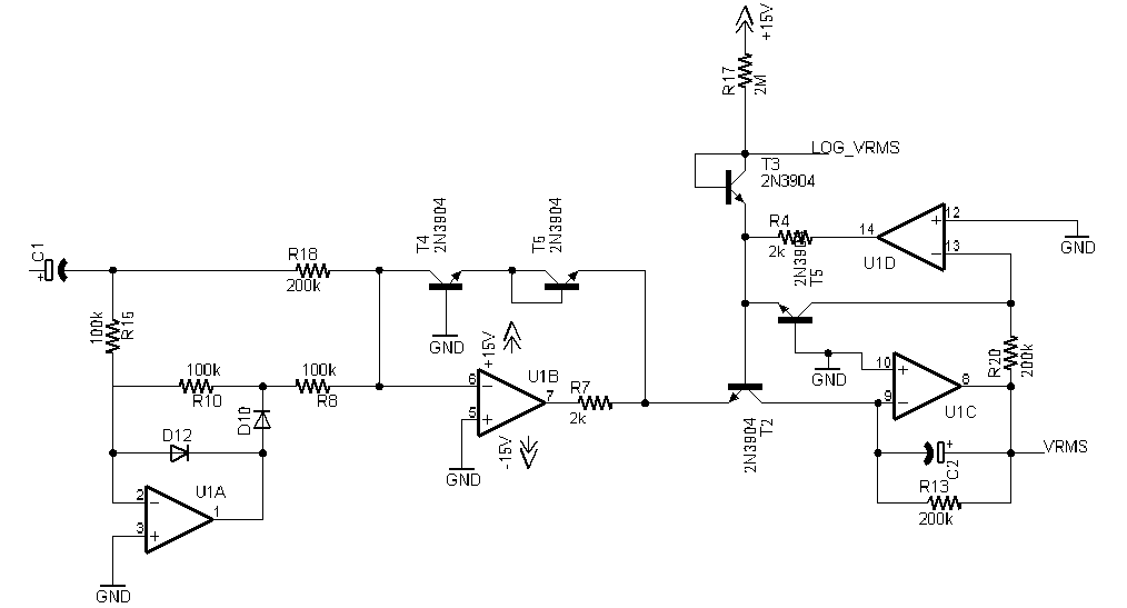
The next opamp stage wraps two Vb-es in the feedback loop to generate 2x LOGx to effectively square the signal.
When this doubled (squared) voltage is applied to emitter of T2 it decodes 2xLogX into the current squared. This current is integrated by C2.
As C2 integrates up, R20 and U1D pulls that integrated RMS current through T5 to perform the square root operation, completing the RMS algorithm calculation.
To be useful for any playing along at home (with VCAs and dB gain control math), I added another Vbe drop to establish a 0VU reference. Transistor T3 is excited by a constant current and when the AC input current equals that static DC current there will be 0Vdc at the node labeled LOG_VRMS. Signals will generate a log voltage on the order of -3.3mV per dB above or below 0VU reference (set by 2M resistor). Note above 0VU signals generate a negative voltage output, below 0VU a positive voltage. This point obviously needs to be buffered and another opamp could easily, scale, buffer, and invert if needed.
To visualize how this circuit works, imagine an initial condition of say -100 VU audio input. All the transistor Vbes are at some small stable nominal voltage, except for T3 our zero reference, so it will have a full 0VU drop across it and be sitting a few hundred mV positive, reflecting the -100 VU.
Next we input a 0VU step function. Immediately T4 and T6 step up to full 0VU Vbe drops. T2 instantaneously draws the 0VU current squared as C2 charges up. As C2 charges the current in T5 increases, increasing the Vbe drop of T5, reducing the Vbe and current in T2. At final equilibrium all of the transistor Vbe are equal, resulting in 0V =0VU. at LOG output, and the actual RMS voltage at U1C opamp output.
I have used variations on circuits like this in meters and sundry applications. I am not convinced the true RMS is all that useful, but it isn't very hard to generate. Also with the circuit I drew up the time constants are very well defined (C2 and R13) and can be easily changed.
JR[/quote]
Wow! John, this circuit is nearly identical to one I used about 20 years ago when designing a couple of feed forward detected multiband processors for a radio station.
To be used in that application, the circuit needs additional time constant circuitry, as integrator filtering alone does not work well, even as a simple stand alone compressor. This really raises the complexity of the circuit, especially when used in multiples in the kind of box I was designing.
I can see why Blackmer and dbx used their circuit: simplicity, repeatable results, and it sounded fairly good for it's intended purpose.


 BX 146221 found in my DBX 224 noise reduction unit and any clear schematic or detail informations