owel
Well-known member
This is my workflow when designing a new Eagle part library.
I like to buy the part beforehand, if possible. This gives me the chance to touch it and visually inspect the part and verify that the part dimensions match the working drawings from the manufacturer.
If working drawings from the manufacturer are not available, I use my digital caliper to make detailed dimensions of the part outline, and pin spacing and pin diameters.
If official PDF working drawings/datasheet are available, I use it though. Trust, but Verify.
Today, we're creating an Eagle part library for a switch.
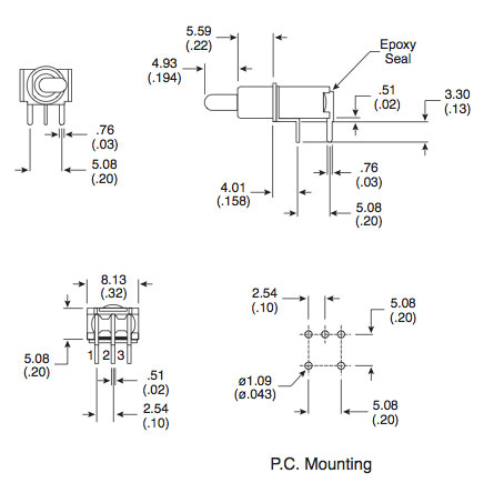
Opening the datasheet, we look for the part dimensions.
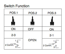
In this case, we also take note of the switch positions, to see which terminals are connected depending on the switch position (up or down).
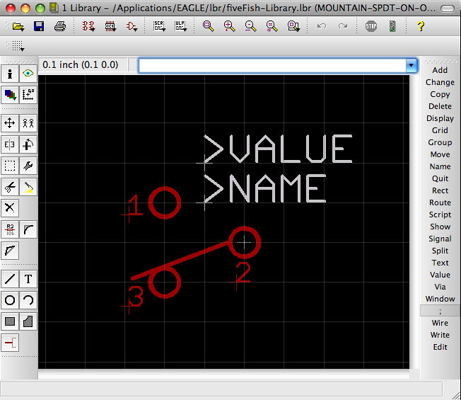
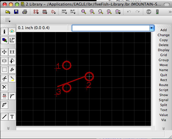
Next step is creating the schematic symbol for the part. In this case, an SPDT switch.
We also add "pins" to the schematic symbol. I use a "point" when defining pins on the schematic symbol.
I also like to match the "pin numbers" with the actual pin numbers used by the manufacturer.... makes life simpler.
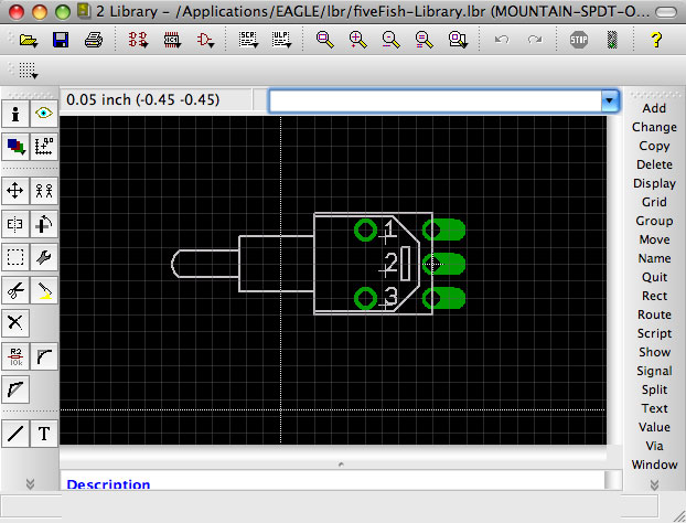
Next, is creating the physical outline of the part. This is the FUN part for me. I like to make the part looking as authentic as possible. We also take care that we're following the part dimensions specified by the manufacturer. Don't forget to check pin spacings, and most importantly... pin DIAMETER. Since the PCBs will have plated through holes, I make the pad diameters just a hair-thin slightly bigger.
To make working easier, make sure to set your snaps and grid to 0.05" square, and 0.01" for the fine grid spacing.
And make sure holes/pads are centered on each "snap."
Make a print out your part and overlay the real part against your "printed part outline." Check if the holes, dimensions are correct and aligned. You may need several passes to get this right if you don't have official working drawings and just relying on caliper measurements.
If everything looks good, then we proceed to the next step.
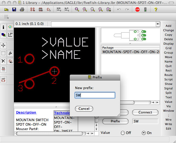
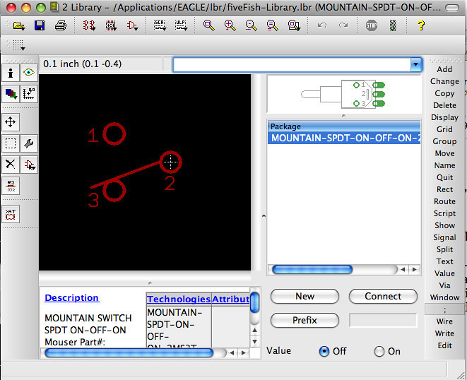
Now, we tie together (match) the pin#s we created in the schematic symbol with the actual pin#s in the part outline.
This is also a good time to enter a part description field. I try to include Mouser or Digikey part #s in the description.
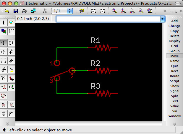
Next step is I try to use the new part library in a test schematic.
I want to verify that when I connect other components to this new part, that the correct pins correspond with the PCB design.
This is a good time to catch any errors you've made in pin-matching.
Here's our test schematic. R1 is connected to terminal #1 of the switch, R2 connected to terminal #2 and R3 connected to terminal #3.
Then we switch to the Board Layout view and verify that it's correct.
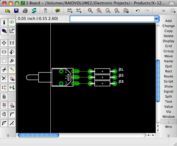
And we see that everything is OK. The pin #s in the schematic match the pin#s in the board layout.
And we're done.
I like to buy the part beforehand, if possible. This gives me the chance to touch it and visually inspect the part and verify that the part dimensions match the working drawings from the manufacturer.
If working drawings from the manufacturer are not available, I use my digital caliper to make detailed dimensions of the part outline, and pin spacing and pin diameters.
If official PDF working drawings/datasheet are available, I use it though. Trust, but Verify.
Today, we're creating an Eagle part library for a switch.
Opening the datasheet, we look for the part dimensions.
In this case, we also take note of the switch positions, to see which terminals are connected depending on the switch position (up or down).
Next step is creating the schematic symbol for the part. In this case, an SPDT switch.
We also add "pins" to the schematic symbol. I use a "point" when defining pins on the schematic symbol.
I also like to match the "pin numbers" with the actual pin numbers used by the manufacturer.... makes life simpler.
Next, is creating the physical outline of the part. This is the FUN part for me. I like to make the part looking as authentic as possible. We also take care that we're following the part dimensions specified by the manufacturer. Don't forget to check pin spacings, and most importantly... pin DIAMETER. Since the PCBs will have plated through holes, I make the pad diameters just a hair-thin slightly bigger.
To make working easier, make sure to set your snaps and grid to 0.05" square, and 0.01" for the fine grid spacing.
And make sure holes/pads are centered on each "snap."
Make a print out your part and overlay the real part against your "printed part outline." Check if the holes, dimensions are correct and aligned. You may need several passes to get this right if you don't have official working drawings and just relying on caliper measurements.
If everything looks good, then we proceed to the next step.
Now, we tie together (match) the pin#s we created in the schematic symbol with the actual pin#s in the part outline.
This is also a good time to enter a part description field. I try to include Mouser or Digikey part #s in the description.
Next step is I try to use the new part library in a test schematic.
I want to verify that when I connect other components to this new part, that the correct pins correspond with the PCB design.
This is a good time to catch any errors you've made in pin-matching.
Here's our test schematic. R1 is connected to terminal #1 of the switch, R2 connected to terminal #2 and R3 connected to terminal #3.
Then we switch to the Board Layout view and verify that it's correct.
And we see that everything is OK. The pin #s in the schematic match the pin#s in the board layout.
And we're done.