>> OK.....that's fine. Now.....I am -- NOT -- bragging here about myself or even anything remotely close, OK??? But, there is a significant difference between a "GERBER Viewer" (especially one that is also provided by the PCB-design program) and my rather expensive and pricey -- INDEPENDENTLY OPERATED -- "GERBER and N/C Drill Data Analysis & Editing" program. Here is an example:
About 16-years ago while working at a high-end video electronics company, I decided to one day install this program I use here-at-home at my job and I loaded in a few sets of the GERBER files that we had sent out previously to have our PCB's fabricated from. You can't imagine how shocked I was looking at my monitor and seeing how "totally screwed up" that these files were!!! So, I called our PCB-fabrication company and I told them what I was looking at. Their response back to me???.....
"Yeah.....your GERBER files are always screwed up like that when we get them from you!!! It usually takes us a little over half-an-hour to get everything to a point where we can fab your boards for you"!!! -- Weird, huh???
So.....I then asked him, "Why haven't you contacted me to let me know this"???
His reply???....."Our job is to provide you with working PCB's, so we go ahead and spend the time to fix your garbage GERBER files and get you the boards that you're paying for. We figure.....if we told you that your GERBER files are total garbage, then you just might go to another fabricator. So, we -- DON'T TELL YOU -- that your files are garbage and just go ahead and fix them as is needed. You pay for it in our increased setup time to prep your files"!!!
>> OK, now.....all of this brings up two points: 1) The PCB's are being fabricated with "garbage" GERBER and N/C Drill data files and, 2) -- HOW IS IT -- that an expensive and top-line industry-leading PCB-design software program can create -- GARBAGE -- output files and NOT be seen? After all.....this expensive PCB-design software program also has its own "GERBER Viewer" within it. Now what?
So, I call the "Tech Support" group at the PCB-design program headquarters and relate to them not only what I have discovered on my own by using this -- independent -- (important detail here) GERBER & N/C Drill analysis program, but also what I have been told by our PCB-fabrication vendor. Of course, they didn't believe me. But, eventually I was able to convince them that "something" has to be wrong with their program because both our PCB-fabricator and I see the same screwed-up images on our monitors and we are also both using different GERBER & N/C Drill data editing programs!!! So.....they reluctantly told me that they would look into the matter. GEE!!! THANKS!!!
About 10-days later the "Tech Support" guy calls me back and tells me this....."We related your issue to our developers and they told us here that what you are telling us "just can't be". However, we insisted that they look into the matter because both you and your PCB-fabricator are seeing the same incorrect data. After the developers looked at and analyzed our program code, they discovered two separate issues. The first issue they found was that there were some lines of code in the output creation files which prevented all of the files from being aligned with one another at their "0/0" datum point. The second issue that they discovered was in the "GERBER Viewer". Because it operates from the same database as the main program files, it works out that even though the GERBER files themselves are totally out-of-alignment and because the "GERBER Viewer" and the PCB-design program both reference the same database, the "GERBER Viewer" displays the images as being correctly in alignment even though they're not. It was because you were viewing the GERBER and N/C Drill files using an -- independent -- program that had no connection to the PCB-design software, you were able to see how the files ACTUALLY ARE. We have alerted our program developers to this newly unknown error and we will be issuing a new software release later on this year"!!! And.....this was an $8,000 "industry-standard" PCB-design program!!!
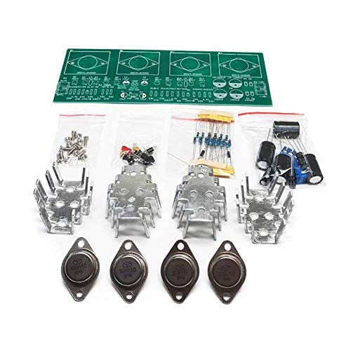
>> So.....go ahead and have your PCB's made. I tried.....
/


![Soldering Iron Kit, 120W LED Digital Advanced Solder Iron Soldering Gun kit, 110V Welding Tools, Smart Temperature Control [356℉-932℉], Extra 5pcs Tips, Auto Sleep, Temp Calibration, Orange](https://m.media-amazon.com/images/I/51sFKu9SdeL._SL500_.jpg)