Bo Deadly
Well-known member
This "SQ-RSEout" PCB is available on OSHPark for ~$10 USD:
https://oshpark.com/shared_projects/Rmc0838n
This tiny 1.8"x1.08" PCB replaces the "filter board" and 1/4" TS jack of the "OUTPUT" of a Roland Space Echo like RE-201 or RE-101. So you basically remove the old filter board and old TS 1/4" jack it's soldered to, disconnect various wires, reconnect some, add one new and then mount this new PCB using the new TRS jack soldered to it.
FEATURES:
SCHEMATIC:
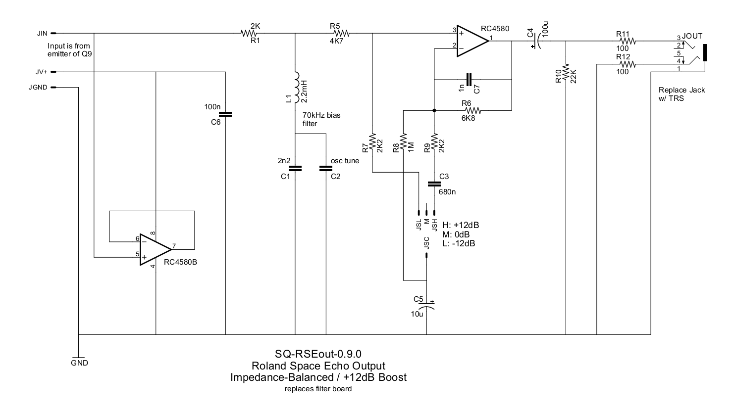
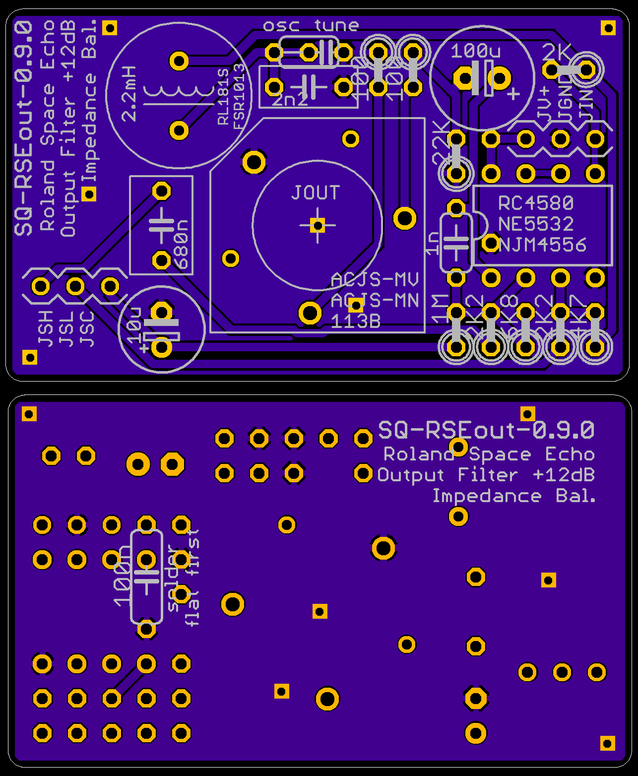
PCB BOARD 1.8" x 1.08":
MODIFICATIONS:
The following graphic illustrates precisely how to integrate the new board:
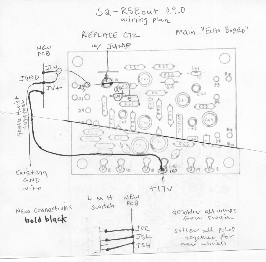
Remove the old "filter board" and all wires from the LMH switch (careful not to apply too much heat to the switch - flux is your friend). Connect the signal wire to JIN, the signal wire ground shield and existing GND wire (will need to redress these wires - more below) together to JGND and then add a completely new wire from solder lug 16 on the Echo Board to JV+ (gently twisting it alongside the exiting GND wire).
To connect the switch wires just run short bits of bus wire (maybe with little bits of insulation). The different poles of each switch position are not used so you can connect them all together (or not).
Here are some example build pictures:
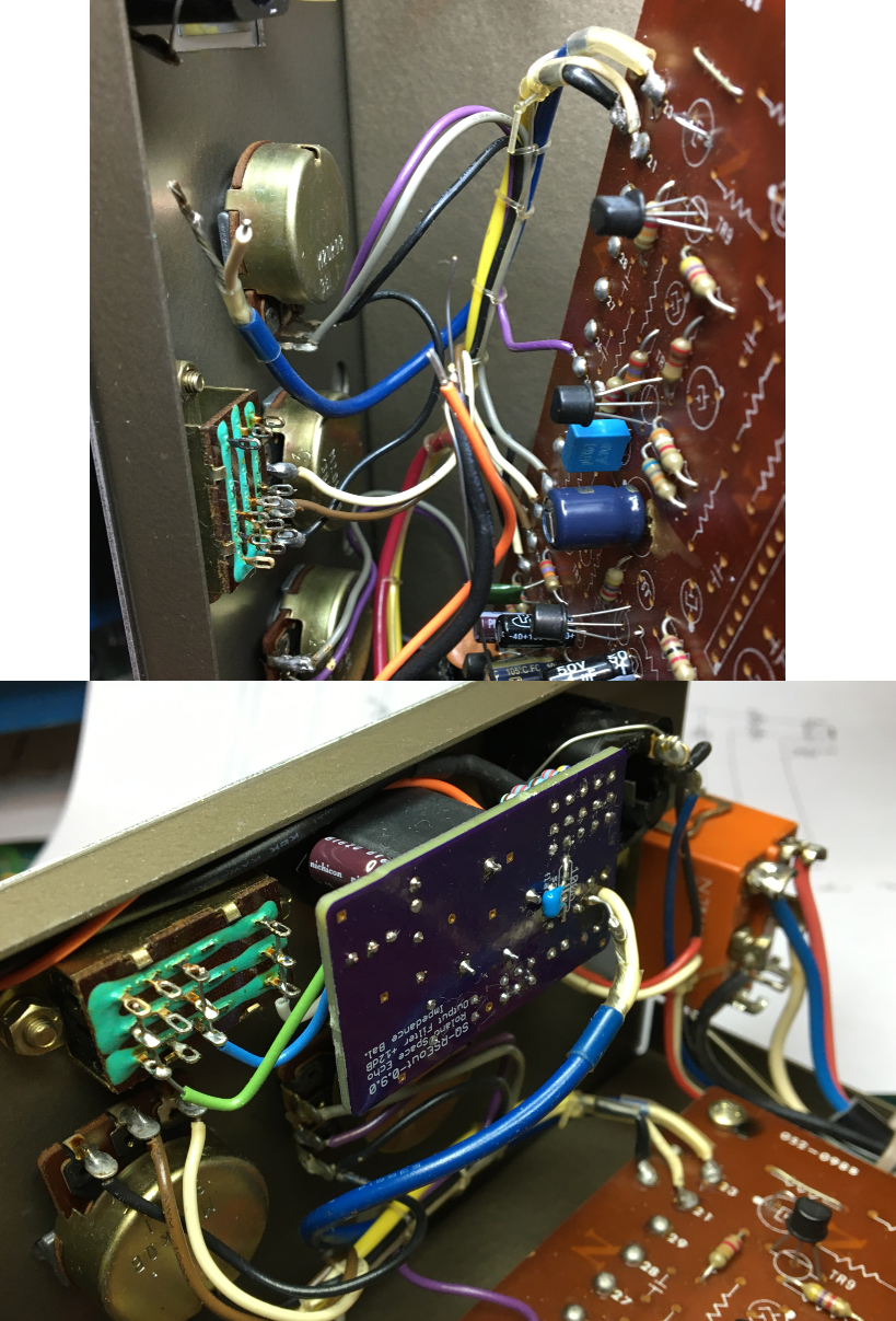
The first pic shows all wires cleaned up and prepped. Specifically, consider:
1) C72 has been replaced with a piece of bus wire. To get to C72, the main board has been lifted up but it is completely acceptable to just solder a small piece of bus wire across the pads if you can lift the board enough without de-soldering any of the wires (or maybe use a razor blade to cut the leads of C72 from the top of the board and strap a piece of bus wire across the top). Otherwise, it may be necessary to desolder several wires around wire lugs / pads 13, 14 and 15 to lift the board enough to work on the underside. Regardless, it will almost certainly be necessary to remove some wire lacing. Take pictures. I actually I installed a make-shift connector to make lifting this board easy.
2) The blue shielded signal wire, the ground wire and all switch wires have been de-soldered and prepped. Trim unclean ends, strip and tin all wires. Note that the ground wires might not accept solder very well so you might need to apply extra heat and use leaded solder with a lot of flux.
3) An orange V+ wire has been added from lug 17 on the main board and paralleled with the existing ground wire. The existing ground wire is far too large to fit in the JGND wire pad so you can barely see (right next to the end of the orange wire) that I wrapped a piece of bus wire around it to extend it.
The second pic shows the new board mounted. But first solder the V+ wire to JV+ and the aforementioned ground bus wire to JGND. Using the extra bus wire of JGND, make a "solder lug" on the other side for the equally thick and hard to solder shield wire of the blue signal wire. Add 3 pieces of bus wire for the switch and use some insulation to keep them from touching each other. Make sure the board is perfectly aligned with the bottom of the chassis so that it does not get damaged when the chassis is installed / removed during maintenance. After the board is mounted, solder the switch wires.
ERRATA:
Do not use ACJS-MV jacks. They will work but are difficult to mount to the panel. The outer washer is too tight and inner isolator and washer cannot be used (although chassis isolation is only really required for the foot switch jack). ACJS-MN would be easier. Not sure about Switchcraft 113B/114B.
The PCB holes for the 1/4" jack pins are slightly too small. You will need to crush them a little with pliers first.
C3 680n is not necessary and should be jumped with a piece of bus wire. The idea was that with the extra gain, it might be prudent to roll-off the lows to increase headroom in the high gain position but this has proven to be not necessary.
https://oshpark.com/shared_projects/Rmc0838n
This tiny 1.8"x1.08" PCB replaces the "filter board" and 1/4" TS jack of the "OUTPUT" of a Roland Space Echo like RE-201 or RE-101. So you basically remove the old filter board and old TS 1/4" jack it's soldered to, disconnect various wires, reconnect some, add one new and then mount this new PCB using the new TRS jack soldered to it.
FEATURES:
Impedance balanced output accepts a TRS 1/4" plug and greatly reduces ground loop related hum when driving a balanced input but works correctly with an unbalanced input and with a conventional unbalanced cable.
The "standard" 100 ohm output with a sturdy op amp like an RC4580 or NE5532 can drive long cables and other gear that requires a low impedance source.
The "H M L" slide switch is used to provide +12dB, 0dB and -12dB output. So +12dB of boost is provided in the H position, the M position is what the H position was and the L position actually attenuates.
The inductor / capacitor filter replaces twin-t notch filter of orignal "filter board". Can be tuned by adding an extra small cap. Twin-t was set for 72kHz but oscillator schem reads 60kHz and I have measured 62kHz in my RE-101. So adding an extra 820p should make 62kHz for example.
SCHEMATIC:

PCB BOARD 1.8" x 1.08":

MODIFICATIONS:
The following graphic illustrates precisely how to integrate the new board:

Remove the old "filter board" and all wires from the LMH switch (careful not to apply too much heat to the switch - flux is your friend). Connect the signal wire to JIN, the signal wire ground shield and existing GND wire (will need to redress these wires - more below) together to JGND and then add a completely new wire from solder lug 16 on the Echo Board to JV+ (gently twisting it alongside the exiting GND wire).
To connect the switch wires just run short bits of bus wire (maybe with little bits of insulation). The different poles of each switch position are not used so you can connect them all together (or not).
Here are some example build pictures:

The first pic shows all wires cleaned up and prepped. Specifically, consider:
1) C72 has been replaced with a piece of bus wire. To get to C72, the main board has been lifted up but it is completely acceptable to just solder a small piece of bus wire across the pads if you can lift the board enough without de-soldering any of the wires (or maybe use a razor blade to cut the leads of C72 from the top of the board and strap a piece of bus wire across the top). Otherwise, it may be necessary to desolder several wires around wire lugs / pads 13, 14 and 15 to lift the board enough to work on the underside. Regardless, it will almost certainly be necessary to remove some wire lacing. Take pictures. I actually I installed a make-shift connector to make lifting this board easy.
2) The blue shielded signal wire, the ground wire and all switch wires have been de-soldered and prepped. Trim unclean ends, strip and tin all wires. Note that the ground wires might not accept solder very well so you might need to apply extra heat and use leaded solder with a lot of flux.
3) An orange V+ wire has been added from lug 17 on the main board and paralleled with the existing ground wire. The existing ground wire is far too large to fit in the JGND wire pad so you can barely see (right next to the end of the orange wire) that I wrapped a piece of bus wire around it to extend it.
The second pic shows the new board mounted. But first solder the V+ wire to JV+ and the aforementioned ground bus wire to JGND. Using the extra bus wire of JGND, make a "solder lug" on the other side for the equally thick and hard to solder shield wire of the blue signal wire. Add 3 pieces of bus wire for the switch and use some insulation to keep them from touching each other. Make sure the board is perfectly aligned with the bottom of the chassis so that it does not get damaged when the chassis is installed / removed during maintenance. After the board is mounted, solder the switch wires.
ERRATA:
Do not use ACJS-MV jacks. They will work but are difficult to mount to the panel. The outer washer is too tight and inner isolator and washer cannot be used (although chassis isolation is only really required for the foot switch jack). ACJS-MN would be easier. Not sure about Switchcraft 113B/114B.
The PCB holes for the 1/4" jack pins are slightly too small. You will need to crush them a little with pliers first.
C3 680n is not necessary and should be jumped with a piece of bus wire. The idea was that with the extra gain, it might be prudent to roll-off the lows to increase headroom in the high gain position but this has proven to be not necessary.


