bcarso
Well-known member
[quote author="clintrubber"]FWIW this T.H.E.-circuit is quite hefty with the nanoFarads as well ...
I guess a manufacturer has to go a bit more for 'sturdy under as many conditions as possible' - at the cost of a bit higher distortion.
Regards,
Peter[/quote]
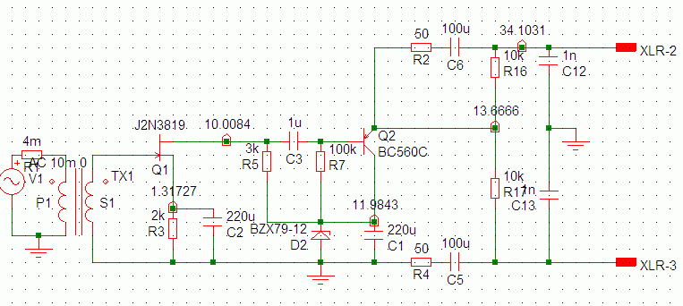
The "phase" splitter approach is tricky, and Samuel is correct in warning of potential distortion effects (although these will likely be fairly small compared to the basic distortion of the FET). At first glance, knowing that collector impedance is much higher than emitter under normal bias, one would expect the high frequency response of + out and - out due to capacitive loading to be asymmetrical. But as mentioned above, because the current that the emitter supplies comes mostly from the collector, if the loading capacitors are equal there is compensation and the measured responses for each line are about the same. But the transistor is working harder.
If there is asymmetrical loading things get a lot different. For example, for the original circuit (the second schematic at the beginning of this thread), if you take away C13, the frequency response at the collector output loaded by C12 at 22nF is down 3 dB at only about 5.1kHz! Restore C13 and the response goes out to over 300kHz. This assumes light loading at the destination.
The double emitter follower approach of the T.H.E. circuit is intrinsically symmetrical, without much interaction due to loading, and the rolloff will be due to the series R plus emitter impedance breaking with the C's.
EDIT: from sim the loading effects on the phase splitter are surprisingly small, and also may induce distortion that tends to cancel some of that coming from the FET.
I guess a manufacturer has to go a bit more for 'sturdy under as many conditions as possible' - at the cost of a bit higher distortion.
Regards,
Peter[/quote]
The "phase" splitter approach is tricky, and Samuel is correct in warning of potential distortion effects (although these will likely be fairly small compared to the basic distortion of the FET). At first glance, knowing that collector impedance is much higher than emitter under normal bias, one would expect the high frequency response of + out and - out due to capacitive loading to be asymmetrical. But as mentioned above, because the current that the emitter supplies comes mostly from the collector, if the loading capacitors are equal there is compensation and the measured responses for each line are about the same. But the transistor is working harder.
If there is asymmetrical loading things get a lot different. For example, for the original circuit (the second schematic at the beginning of this thread), if you take away C13, the frequency response at the collector output loaded by C12 at 22nF is down 3 dB at only about 5.1kHz! Restore C13 and the response goes out to over 300kHz. This assumes light loading at the destination.
The double emitter follower approach of the T.H.E. circuit is intrinsically symmetrical, without much interaction due to loading, and the rolloff will be due to the series R plus emitter impedance breaking with the C's.
EDIT: from sim the loading effects on the phase splitter are surprisingly small, and also may induce distortion that tends to cancel some of that coming from the FET.