Hi,
PCB has a plane on both sides that is tied to CHASSIS connector. Signal and Power grounds have separate pads.
As far as PIN1 selection I did it only for input. In my builds I skip it all together and just solder PIN1 to chassis, but if you're using some legacy equipment you may want to have the molex header over there. The other goldpin on the board is LINK selection. You can link all 8 modules if you want to
Regards,
Michal




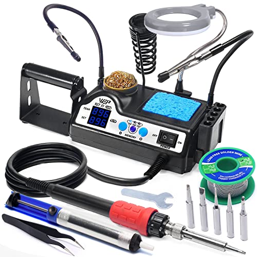
![Soldering Iron Kit, 120W LED Digital Advanced Solder Iron Soldering Gun kit, 110V Welding Tools, Smart Temperature Control [356℉-932℉], Extra 5pcs Tips, Auto Sleep, Temp Calibration, Orange](https://m.media-amazon.com/images/I/51sFKu9SdeL._SL500_.jpg)
