DCBloak on the bench...

GroupDIY Audio Forum

Help Support GroupDIY Audio Forum:

This site may earn a commission from merchant affiliate links, including eBay, Amazon, and others.

hifizen

Well-known member
Joined
Apr 6, 2006
Messages
51
Location
Silicon Valley, CA
Continued from "Another Bloak Hack..." thread in the drawing board section, now that the circuit is up and running on my workbench.

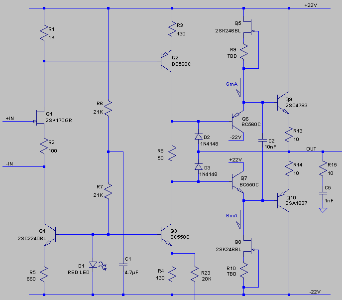
As mentioned, my idea was to start with tk's excellent BigFetBloak circuit, and modify it a bit for use in a hi-fi stereo. My goals were to provide for DC (or transformer) coupling with a servo if needed, headphone drive capability, and gains down to unity, while retaining the simple nature of the original as much as possible. A big thanks to bcarso, Samuel Groner and others who contributed design ideas in the drawing board thread. I think one of the best ideas to come out of that discussion was the diamond buffer for the output. There are still some minor details to sort out in the temperature compensation / servo and noise areas, but that will come later. For now, I'd like to present my results with the diamond buffer...

Here's the prototype, pretty much as built:
DCBloak_r0_2g_schem.gif


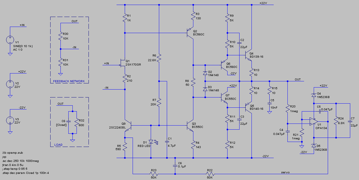
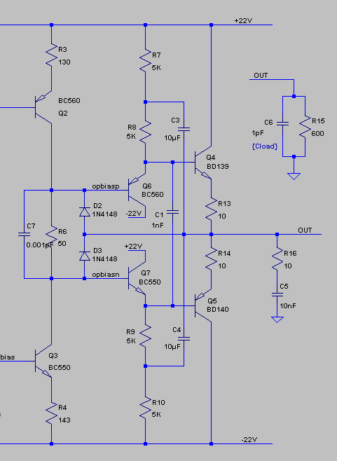
There are a few differences from the schematic as shown... I did not build the servo section, so R5 is more like 660 ohms (actually a trimpot for now, but trimmed to almost exactly the 660ohms LTSPICE predicted). I also substituted 2SC4793 / 2SA1837 transistors instead of BD139 / BD140 for the output (great specs, and about 50c each from Digikey). I used only a 1nF cap in the output Zobel, since I didn't have a 10nF film easily on hand, and I wanted to see how it would behave without as much Zobel damping.

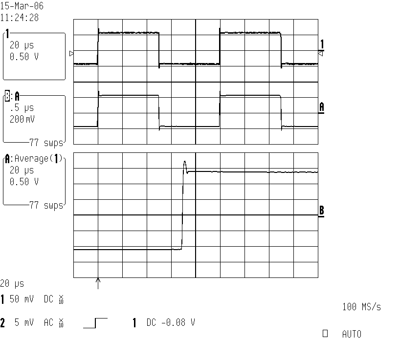
The diamond buffer was tested open loop by grounding the +IN node, omitting the feedback network, and injecting signal directly at the Q6 base with a function generator.

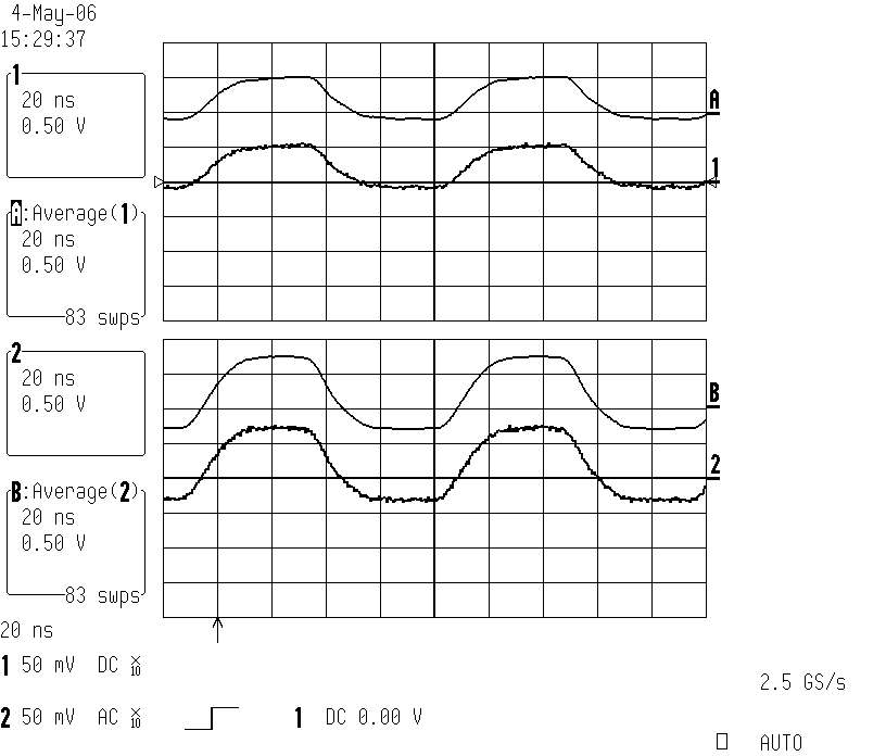
100kHz square wave response looked promising:
cap003.png


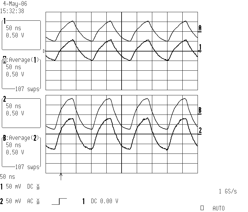
But as I mentioned in the old thread, sine wave response collapses into a distorted triangle wave at about 7MHz. Trace 2 shows the input waveform measured at Q6 base:
cap007.png


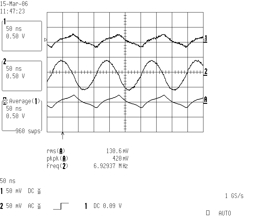
The input signal is only mildly distorted as this is happening - it still basically looks like a decent sine wave. In order for the stage to recover, the frequency has to back off all the way down past about 4MHz. I'm not entirely sure why this frequency hysteresis effect exists.

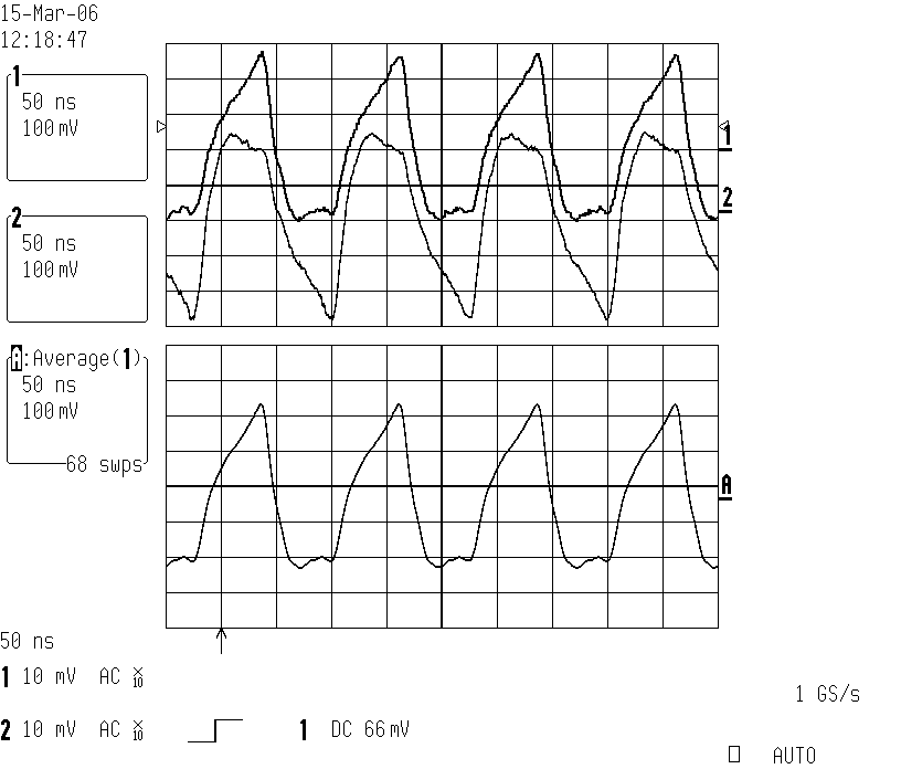
For a better look at what's going on, I measured waveforms at Q6 and Q7 emitters. This capture shows the output waveform at 8MHz (trace 1, averaged version at A), and the Q6 emitter waveform (trace 2"):
cap010.png


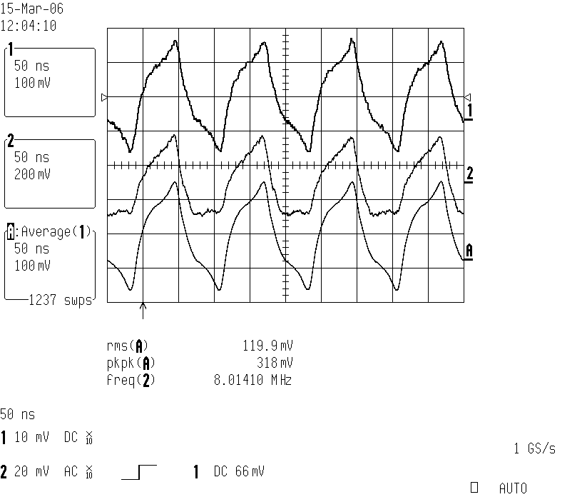
and this one shows Q6 and Q7 emitter waveforms at the same time:
cap012.png


My thought right now is that Q6 and Q7 are not running at a high enough standing current, and are running out of steam at high speed. Due to the loading problem presented by the bootstrap arrangement, I've decided to try switching to FET current sources instead to see how that does. I'll start off at about 6mA for each driver, and increase from there if necessary.

Any further insight into what's going on with those waveforms would be most welcome.
 
What happens to d.c. levels during the "sine wave collapse" phenomenon episodes?

Often in highly asymmetrical topologies like this, what amounts to a modest effect, generating some second-harmonic distortion and an associated d.c. offset, becomes a fatal increase in both at high frequencies. Of course you could prudently limit the bandwidth right at the input, but I realize you would like to see what the naked amp does by itself with anything you can throw at it.
 
DC level didn't seem to do much if anything... the trace showing the diamond buffer's output was DC coupled for all the measurements shown, and I didn't adjust DC level on the function generator between the square wave test and the sine response test. Only the Q6 / Q7 emitter waveforms were AC coupled. So, if there was an accompanying DC shift, it looks pretty small to me. I'll run the test again and try and keep a close eye on the trace to see if it offets suddenly when the sine collapses (it's quite sudden as the frequency goes up - clean sine... clean sine... then *bam* ... distorted output).

By the way, just on a whim, I tested the closed loop response as well... just a quick peek. I used a single 10K feedback resistor to set unity gain. Square wave response looks not too shabby, with a little ringing (maybe 2.5 cycles of roughly 10.8MHz before it damps out), very symmetrical on both the pos. and neg. edges. I'll upload another waveform if anyone's interested.
 
Yup. Interestingly, I can duplicate this effect in LTSPICE. What's odd is that the .ac analysis shows a flat response out to over 50MHz... Should it not show at least a 3dB dip at around 10-ish MHz? I had to go back and do a .tran analysis and crank up the input frequency to see this distorted waveform, but it looks remarkably accurate to what I observed on the bench. Better correlation with reality than I would have expected from spice. On the other hand, as I crank up the frequency in spice, I see a gradual decline from a clean waveform into a progressively more and more distorted waveform, whereas in real life, the collapse happens suddenly, with this strange hysteresis thing going on.
 
Rails look pretty clean... perhaps about 10mV little ripples, but then again, the prototype has fairly minimal decoupling on the board (47uF + 0.1uF per rail). The final thing will have a larger 'lytic in there.

Generator output is 50ohms, although I don't think it's being loaded too much. See 2nd screen capture above, trace 2 - this is the input waveform measured at the function generator's point of injection into the circuit (Q6 base / top of R8). I see some loading but not enough to be of serious consequence.

Last night I changed out the bootstraps for a pair of 2SK246BL FETs, CCS-strapped. These measured Idss of a hair over 7mA at room temp, and in practice ran at about 6mA (I installed some 10R resistors to monitor). At first this seemed to take care of the issue (at least up to 13.5MHz, the limit of my function gen), but I noticed as the FETs warmed up and their current decreased, the problem returned, albeit at a higher frequency. So that didn't fix it.

However, having successfully duplicated the problem in SPICE, I started fiddling around, and I think my original understanding of the problem is correct. In sim, the driver transistors are clearly going into saturation, trying to drive the output device's Cob (even though it's only 20pF or so, and we don't have Mr. Miller to worry about). Esox suggested a cap between the driver emitters, and in sim this fixes the problem... it allows the opposite driver transistor to source current into the active output's base when it's own driver cuts off. Another way of looking at it is that the emitter coupling cap allows push-pull drive into the output transistors at high frequencies. Here's what it looks like (C1 is the important cap, C7 was an experiment, doesn't turn out to be very useful):

DCBloak_r0_2g_capfix.gif


Next step is to try this cap in real life and see how it does. Stay tuned...
 
Now that you mention it I've used a similar arrangement before, although I started off with R's in the driver Q emitters to produce the offset that's being done in your arrangement with R6. Then I added two Cs with small Rs in series (to quell parasitics) to cross-couple the driver emitter to same-sex output base. I'm not sure that there was any advantage to that compared to your arrangement. I usually use bipolar current sources with LED or two-diode bias in lieu of the bootstrapped Rs.

I think your analysis is about right, except that it is not as much the ~20pF Ccb of output devices you are fighting, as it is the output load of 10nF with some series R---the rough transformation for what the driver sees is the available current gain (1+beta for a common-collector stage) at a given frequency dividing the 10nF and multiplying the Rs. With ~50MHz f sub t output devices you only have around a factor of 6 reduction of the output load at 10MHz for example. Probably the bootstrapping arrangement exacerbates that effect and the "collapse" effect a bit as well.

Also, without the crosscoupling, the driver transistors can at most cut off and leave the bootstrapped 5k's to supply the output Q bases.

EDIT: Also note what happens to the input Z of the whole buffer when things run out of steam, and the effect this has on the open-loop gain vs. frequency of the whole shebang.
 
[quote author="bcarso"]I think your analysis is about right, except that it is not as much the ~20pF Ccb of output devices you are fighting, as it is the output load of 10nF with some series R ... With ~50MHz f sub t output devices you only have around a factor of 6 reduction of the output load at 10MHz for example.[/quote]
That's a good observation - it's quite likely a contributing factor. Some follow-up in SPICE may be a good idea.

Have a look at what happened when I added 10nF across the driver emitters... keep in mind, this is with the 2SK246 JFET current sources (6mA each) instead of the bootstraps, but I bet the effect would be pretty much the same. This is at 10.6MHz, just past the point of 'collapse'. Trace 1 shows the output, trace 2 is the driver emitter:
cap023.png


And here we have the same nodes observed at 8MHz, as I bring the frequency back down toward the point where it snaps back into proper non-distorted operation (which occurs at about 7.1MHz in this circuit configuration):
cap024.png


Looks a lot like a series of RC charging exponential curves to me...

I think what I found most interesting is when I measured the DC voltage across that cap... in normal operation, I measure about 1.6V there... the 0.35V across R6, plus the two Vbe's of the drivers. As soon as the waveform collapses, this drops to about 0.75V. Something is obviously sucking enough charge away from the driver emitters that they are unable to recover to their normal operating point within a single cycle. I figure what might be happening is a sort of 'rectification' effect, whereby the driver transistor can sink (in the PNP case) large currents when 'pulling', but goes into cutoff when 'pushing' (limiting the 'push' current to that of the CCS)... it becomes (to some extent) a one-way current gate, giving asymmetric drive into the output transistor's base. The bias across the output devices collapses, and they go into class-B. Meanwhile the driver stage is unable to provide enough current into the outputs to recover to their normal operating point. Thus, the condition persists down to a lower frequency than it started at, until there is sufficient time available within a single cycle to recharge the base capacitance and/or drive the load back up to the drivers' normal operating point. When you reach that point... *pop* ... the stage recovers to it's intended bias point, and the output returns to a clean sine wave.

Did that make sense? I guess my ponderance at this point is whether the emitter loading is capacitive or simply due to low beta at high frequency, combined with the Zobel's loading. One other note worth repeating at this point, since it isn't reflected in the schematic ... my prototype's Zobel is 10R/1nF, not 10R/10nF.

[quote author="bcarso"]Also note what happens to the input Z of the whole buffer when things run out of steam, and the effect this has on the open-loop gain vs. frequency of the whole shebang.[/quote]
Fortunately, I don't intend to pass anything other than audio through this little guy, but just in case it gets hit with NPR or AM1060, and because I like to see a nice clean step response and wide b/w before closing the loop... I'll chase this one down till I feel it's understood well enough to say with confidence that it won't be an issue.
 
Here's a more accurate schematic of what I'm actually measuring right now:
DCBloak_r0_2i_schem_partial.gif


I renumbered a lot of parts, since the numbering had become encumbered with the numerous intervening changes, so part designators are no longer consistent with my earlier versions of the schemo. Also not visible here is the servo portion of the schematic, which I haven't built yet anyway. But note where the servo point is... servo feedback comes in bottom-center in the schematic, through R23.
 
OK, it has been a couple of weeks since my last post... time for a brief update:

I've completed testing on the output buffer and other amplifier stages and progressed through closed-loop testing and tweaking as well. I'm not quite ready to post the completed project schematics yet, as the servo portion is not complete and there is still some optimizing to do, but the AC performance of the main circuit is looking very good, and I'm quite satisfied with it at this point. Frequency response, output swing, clipping behaviour, current limiting, and operation into very low impedances (I tested right down to 25ohms) and capacitive loads is all looking excellent. A noise and subjective sound quality test with headphones is all that remains (will have to wait until the DC is sorted out), but I expect the performance here to be exemplary as well, given the very quiet JFET input, and the reputation this basic configuration has already garnered.

However, the non-servo'd DC performance is not at the level I was aiming for. Although my simulations have all shown remarkable correlation with the real-world results, and the overall DC drift range over temperature is pretty much what I expected (tested with the aid of a refrigerator and a hair dryer), what I had not expected was the very short thermal time constant and random drift I'm seeing in the sub 2Hz range. This circuit simply likes to drift around a lot... and quickly. It definitely doesn't like any air movement in it's vicinity, so keeping it well enclosed and protected from random air currents would be well advised for getting optimal DC performance from this circuit.

My original servo design placed the corner frequency way down at 0.02Hz, which is where I like it. Combined with a second-order rolloff into the audio band, this ensures that the servo system will be well and truly inaudible, accomplishing what cannot reasonably be done with just a simple coupling cap. But, designing a servo system to keep such large, rapid DC drift reigned in without intruding on the audio band is proving a challenge. It's a fine balance, and I suspect the end result will still, in some cases, suggest an output relay to allow the servo a few seconds at turn-on to stabilize before connecting the load.

I'll build the servo circuit tonight, and test / refine over the next week or so, depending on how much time I have. When it's all done, I'll post the full schematic with my notes and some more waveforms for the curious.

Almost there...
 

Latest posts

Back
Top