The input stage based on the Dan schemo... PCB will be on top of the 1632 PCB
Any opinion about OPA1632 for D/A output amp? ???
Any opinion about OPA1632 for D/A output amp? ???


") Let's say that Input board is solved with few options to try and measure in the real life. What about output DA section?
Let's say that Input board is solved with few options to try and measure in the real life. What about output DA section?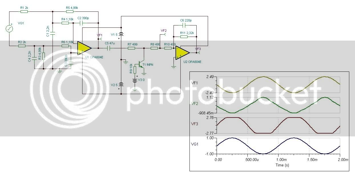
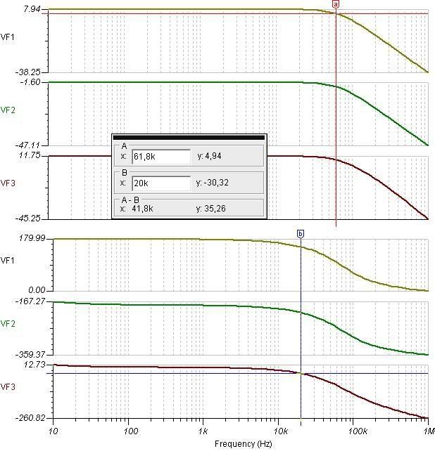 . My comments about crossover and headroom are out of question now but I'm still looking about improving this stage. Cool about moving -3db point , changing tr mute to relay, what can I do more?
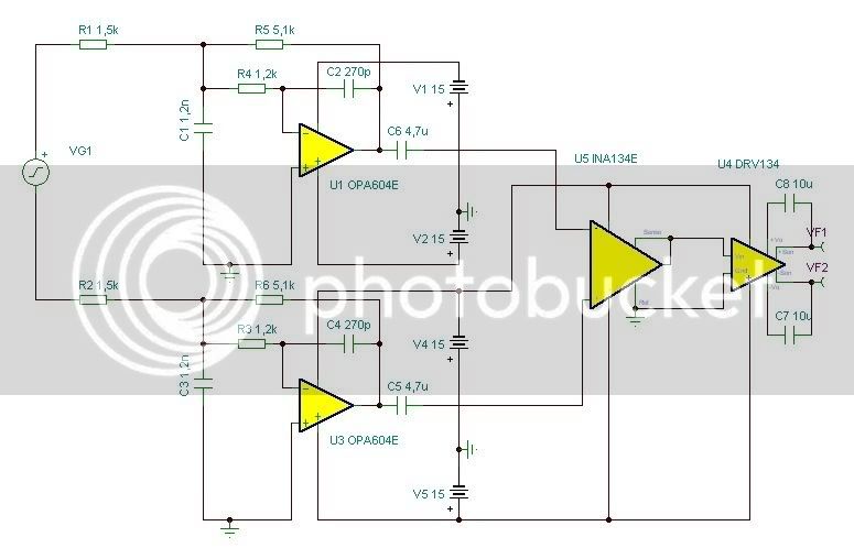
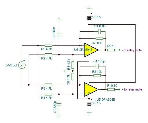 Well it works somehow but since I'm not sure how I will stick to your recommendations. Than, forget about previous schemo, and please tell me (if you find some time) what can I do about this? Of course , all comments are welcome. BTW, I found the way to purchase THAT chips so it's welcome too
 dmills said:There are in any case plenty of good DAC output designs out there, it is in most ways a far simpler thing to design then the input stage.
As ever, board layout makes a huge difference and you will want to get the (if appropriate) current to voltage stage and first filter very, very close to the DAC chip.
Do not get fooled by the presence of Agnd and Dgnd pins on mixed signal converters by the way, for most parts you want them connected to the same ground plane (The issue is bond wire inductance), and remember that converters are high frequency (RF) devices with clock edge harmonics well into the VHF region.
Regards, Dan.

![Soldering Iron Kit, 120W LED Digital Advanced Solder Iron Soldering Gun kit, 110V Welding Tools, Smart Temperature Control [356℉-932℉], Extra 5pcs Tips, Auto Sleep, Temp Calibration, Orange](https://m.media-amazon.com/images/I/51sFKu9SdeL._SL500_.jpg)