DCX2496 audio mod

GroupDIY Audio Forum

Help Support GroupDIY Audio Forum:

This site may earn a commission from merchant affiliate links, including eBay, Amazon, and others.
I decided to try this one. Well , it looks OK in simulation from all aspects. I wonder what you are think about it. I excluded input choke from sim but it will be on the PCB, cap and diodes will be mounted on the ADC board. Of course , PSU caps are excluded from sim too but will be on the PCB .
BEIS1632.jpg
 
Moby said:
.. it looks OK in simulation from all aspects ..

C5 and C8 lpf at 25.6kHz with phase 38° at testfreq.20kHz ? 47pF might be a better fit.
C2 and C7 lpf at 66kHz with phase 16.8° at testfreq.20kHz ? 270pF might be a better fit.
C3 and C4 is a little on the high side. A 470pF drops this lpf to 280kHz.
Isn't the reference for R11,R12,R17,R18,C2,C7 missing ?


edit: exchanged @ with at to not confuse mailprogs.
 
Harpo, your are right. I uploaded the wrong one schemo. This front stage was one I tried before when I wanted to go dirrectly to ADC without 1632 so reference was DC offset  :-\ I changed the pic now including some corrections you suggested. Now when I think twice I'm not sure is it any better than previous (simpler) versions  :-[
BEIS1632-1.jpg
 
For people who does not understand Audio ADC buffer design secrets (like me) here's the good reading  :)
http://www.audiodesignline.com/howto/210605596;jsessionid=N4V55CDIXSEYMQSNDLPCKH0CJUNN2JVN?pgno=1
pdf version : http://www.eetindia.co.in/STATIC/PDF/200901/EEIOL_2009JAN22_INTD_TA_01.pdf?SOURCES=DOWNLOAD
 
After reading this document and listening the suggestions from more experienced guys from here I found that I have to be careful about choosing right value for CL in conjunction  with R1 and AK5393 ADC chip. Can somebody here help about it? Here is quote from reading.
A/D converters manufacturers typically recommend values for R1 and CL. The recommended capacitance of CL is typically on the order of a couple of magnitudes larger than that of the sampling capacitor.This is partially to ensure that there is sufficient charge on CL to prevent a significant voltage drop when the sampling capacitor is charged. However, the exact value is often selected via a series of experiments to determine the optimum value for best performance.
InterfacetoaudioADC.jpg

Here are the values from AK5393 data sheet.Should I consider that like AKM recommendation ???
AK5393.jpg

They are "playing" with two values 10n and 1.5n of course with appropriate resistor values. Now what to do? Example 2 looks better for me if the 1632 can drive it, and if I understand it can. Or the truth is somewhere in between? Unfortunately I can't do the "series experiments" like reading suggest  :-\
 
my last post partly lost a little sense with your changed schematic.
If you keep this, maybe some cap changes:
C10 and C11 at 10uF seems enough.
Increase C5 and C8 to 470pF. A 2,8MHz rolloff doesn't make sense.
With -12.7dB in opamps and U-pad your max.level @input would be 22.8dBu or 21.3dBu without R23.
With R3+R4 @ 100r each, C6 @ 2n7 or 3n3 might fit better.
Consider keeping the diodes. You already decreased the series resistors R3/R4 and >10mA input current or turn on spikes might kill your ADC.
Unconcerned if getting the VCOM from AK5393 pin 3/26 to a buffer instead of the voltage divider R5/R7 might be an improvement.
(I still don't like this input stage).
 
Thanks Harpo  :)
my last post partly lost a little sense with your changed schematic.
You are right, I will bring back the wrong schematics and post the "corrected" one after.
With -12.7dB in opamps and U-pad your max.level @input would be 22.8dBu or 21.3dBu without R23.
With R3+R4 @ 100r each, C6 @ 2n7 or 3n3 might fit better.
As I mentioned in previous post that's the part I really don't know how to determine. I understand the current flow but really don't know right value for C6. How did you calculated 2n7 or 3n3? Based on personal experience, or from AKM sheet? Or you have some formula for that? I would like to learn.
Consider keeping the diodes.
Of course, they are not on this board , they will be mounted near the ADC chip together with "C6" (CL).
Unconcerned if getting the VCOM from AK5393 pin 3/26 to a buffer instead of the voltage divider R5/R7 might be an improvement.
It's possible but it have to run through wire 10cm long. That's the only possible distance from new analog - DSP (ADC) board. Is that a problem?
(I still don't like this input stage).
I think that post all my ideas about  :-\ Unfortunately THAT is out of question, and only topology I didn't tried is http://www.dself.dsl.pipex.com/ampins/balanced/balfig13.gif  . To be honest I'm not sure does it make sense to go out of diff mode. I believe that you don't like the input stage, I'm not in love with any of posted too. Can you suggest something besides THAT?
 
Moby said:
With R3+R4 @ 100r each, C6 @ 2n7 or 3n3 might fit better.
As I mentioned in previous post that's the part I really don't know how to determine. I understand the current flow but really don't know right value for C6. How did you calculated 2n7 or 3n3? Based on personal experience, or from AKM sheet? Or you have some formula for that? I would like to learn.
Simple R/C filter. -3dB lpf=1/(2*pi()*(R3+R4)*C6). AKM examples roll off @ 361kHz for the 2*22r/10nF or 295kHz for the 2*180r/1.5nF.
With your 2*100r series resistors the shunting cap 2.7nF set this roll off @ 295kHz. Alternative 3.3nF @ 241kHz because your feeding stages are also limited to this margin.
Unfortunately THAT is out of question, and only topology I didn't tried is http://www.dself.dsl.pipex.com/ampins/balanced/balfig13.gif  . To be honest I'm not sure does it make sense to go out of diff mode. I believe that you don't like the input stage, I'm not in love with any of posted too. Can you suggest something besides THAT?
Maybe a SSM2143 or INA137 as a drop in replacement is easier to source for you if you can't get a THAT1246. Receiver pin1 tied to 0V or a servo stage, though I wouldn't expect much offset if any, output to inverting input of OPA1632 as before with non inverting input tied to 0V.
Something like this maybe.
 
Simple R/C filter. -3dB lpf=1/(2*pi()*(R3+R4)*C6). AKM examples roll off @ 361kHz for the 2*22r/10nF or 295kHz for the 2*180r/1.5nF.
With your 2*100r series resistors the shunting cap 2.7nF set this roll off @ 295kHz. Alternative 3.3nF @ 241kHz because your feeding stages are also limited to this margin.
So simple calculation? From the readings I found I figured that it's much complicated. Correct me if 'm wrong but I understood things like this: "The function of the series resistor  and the load capacitor  between the op-amp and the sampling network has several functions. Capacitor provides the instantaneous current for the sampling capacitor , while the average current is supplied by the operational amplifier. That helps OPA1632 to provide transient current seen by the op amp and the and without that R/C 1632 will ring or overshoot. The resistor isolates the amplifier from the transient currents and also provides the stability required to drive the large capacitive load presented by C. In addition, the combination of R1 and CL provide the required single-pole anti-alias filter and that part you calculated but I think that you have to include value of ADC sampling capacitor. Now my brain hurts because on top of that the time constant of the RC circuit must be small enough to allow the load capacitor to properly charge and accurately reflect the analog input signal and important part of that is that too big value of R  directly translate to distortion." If that's correct than I miss value of the sampling capacitor and I have to trust BB that 1632 is capable to drive capacitive loads of few nf  :-\
 
Moby said:
So simple calculation? From the readings I found I figured that it's much complicated. Correct me if 'm wrong but I understood things like this: "The function of the series resistor  and the load capacitor  between the op-amp and the sampling network has several functions. Capacitor provides the instantaneous current for the sampling capacitor , while the average current is supplied by the operational amplifier. [...]

This is true if the input structure of the ADC is the same as that guy from Cirrus showed in the AudioDesignGuide paper you linked to earlier. I have seen no evidence of that for the AK5393 (in a brief glance through the data sheet). Nevertheless a higher capacitance here in the antialias filter doesn't hurt, as long as it isn't high enough to cause distortion due to higher op-amp loading.

Moby, I feel that you're making this circuit very complex, and I see the same discussions/suggestions appearing several times in this thread. Why do you feel you need three stages to drive the ADC? As there's no global feedback, extra stages have a high likelihood of adding distortion and/or noise. You are determined to use the OPA1632, fine, that's your choice, and you feel in its standard config its input impedance is too low for your passive attenuator. So add either a buffer stage or a diff in-amp (either THAT, or use a simple one-opamp diff in stage like the Beh schematic has around IC7a/b). What's the purpose of having both?

JD 'KISS' B.
 
Yep, one opamp 4*10K resistors, drive the 1632 single ended, job done.
Sure there are better ways to do this, but the above will get it done as long as conditions are not too nasty.

Harpo, I think your gain calculation is wrong, that U is not a pad in any real sense as the feedback for the 1632 is taken from the far end of the build out resistors (at low frequency) so those resistors are inside the feedback loop. I see no need for R23 as it has little effect on anything that I can see.

I will try to draw the way I would do it tomorrow and post that for you lot to pick apart.

Regards, Dan.
 
This is true if the input structure of the ADC is the same as that guy from Cirrus showed in the AudioDesignGuide paper you linked to earlier. I have seen no evidence of that for the AK5393 (in a brief glance through the data sheet). Nevertheless a higher capacitance here in the antialias filter doesn't hurt, as long as it isn't high enough to cause distortion due to higher op-amp loading.
Of course we don't know exact internal structure of the AKM chip but here's the sheet from Cirrus with direct AK-CS conversion.
Code:
http://www.cirrus.com/en/pubs/appNote/an232-1.pdf
To cut a long story short, author claims that ADC buffer from AKM sheet works with CS, so I presume that ADC input architecture is same or similar.
But , buffer they recommend looks different from AKM so I try to figure out analogy between buffer output  RC values. 91ohm/2.7n , 22ohm/10n and 180/1.5n/100ohm.
Moby, I feel that you're making this circuit very complex, and I see the same discussions/suggestions appearing several times in this thread. Why do you feel you need three stages to drive the ADC? As there's no global feedback, extra stages have a high likelihood of adding distortion and/or noise. You are determined to use the OPA1632, fine, that's your choice, and you feel in its standard config its input impedance is too low for your passive attenuator. So add either a buffer stage or a diff in-amp (either THAT, or use a simple one-opamp diff in stage like the Beh schematic has around IC7a/b). What's the purpose of having both?
Yes it turned to complex at the end  :-[ But if you remember I asked can I drive ADC directly because I like it simple. OK , than I learned something with a big help of you guys and than I stacked. I don't have a problem to be stacked because all this writing-reading have besides practical, educational purpose too. No 3 stages, that's definitely wrong approach, but yes, I need reasonably high Z in and I want to drive it balanced. Nothing special about it, I think that most of studio guys need similar thing. Also, I really don't need InGenius CMRR because I have 2.5m from pot to amplifier. At last I can mach resistors to 0.1% and make it acceptable  ;).
So, I will go with opa's2604 non inverting unity gain stage + 1632 but It will be nice to know that mysterious RC in front of AKM.
Yep, one opamp 4*10K resistors, drive the 1632 single ended, job done.
Sure there are better ways to do this, but the above will get it done as long as conditions are not too nasty.
Dan, I would really like to see your drawing.  :)
 
Ok, this is a quick and not particularly well optimised try at what I would probably do.

ADC input.jpg


How it works (and some discussion of compromises):

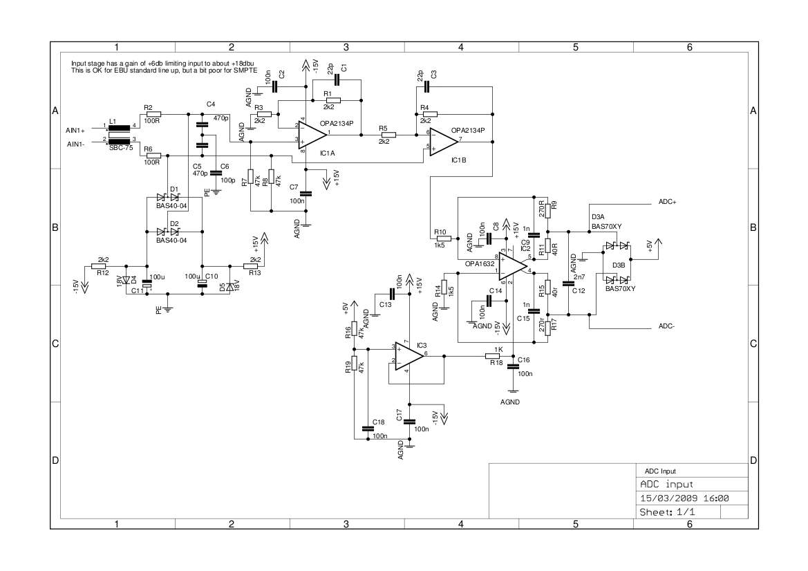
After my normal common mode choke, the input hits an input protection network R2 R6, D1, D2 and associated parts. R2 and R6 serve to limit transient currents but must be kept fairly small to avoid unbalance here spoiling CMRR and to avoid their thermal noise contribution degrading SNR unnecessarily.
The capacitive filter to remove RF around C4 C5 & C6 is set up to minimise the damage to CMRR and common mode impedance due to cap tolerance, common mode will be dominated by C6 which will reduce the effect of tolerances in C4,5 converting common mode to differential mode.  

Note that PE should be a low impedance connection to the case and should not be a mile long connection back to the star point, get it close to the input connector.

As a high input impedance was part of the design brief, I punted for a superbal stage which can have almost arbitrarily high input impedance  (Set by R7 and R8 here), note that the noise floor will probably be dominated by these when the input is O/C.  The single opamp approach suffers badly when you make the resistors large as the resistor thermal noise is unavoidably in series with the input, so the extra opamp was worth it in my view.

R1,3,4 & 5 need to be matched for good CMRR, these could probably be made a little smaller to improve noise performance at the cost of loading the opamps more heavily, but 2K2 feels like a reasonable sort of compromise.  This input stage suffers from always having a gain of 6db, which would be a problem is trying for an input stage suitable for the SMPTE alignment of +4dbu = -20dbFS (implies full scale at +24dbu) as the opamps would run out of headroom and clip.

The output of this stage is then fed single ended to the 1632 stage, which is biased to 2.5V by IC3 and associated components. With +2.5V bias there will be a standing current of a little over a mA flowing in the input resistors which should not be a problem.

Note that all this is DC coupled, mostly because I could not find a good place for a blocking capacitor (A general issue with low Z audio circuits, you need big ones), 10uf in series with each input would be possible, it depends on the application.

The 1n caps (C9,15) at the output form a low pass filter in combination with the feedback resistors (R9,17) which is -3db at about 500Hkz. These caps are required for opamp stability anyway, I just made them larger then would otherwise be required.

Go ahead and shred it!

Regards, Dan.


Dan, thanks a lot  :) Looks interesting. Only thing bothers me is constant +6db gain of input stage driving 1k5+1k5. I believe that noise is small but does it sounds OK? I don't have a problem with 1632, it sounds like it sounds, but with OPA2134 or similar. Sorry if I asked dumb question  :-[
 
You cannot do much about the 6dB gain without screwing up the input impedance (or adding a third opamp), and yea picking an opamp with reasonable output drive would be a good idea, the 2134 was just the first dual part I came across in the part library.

I have no idea how it sounds (or even if it really works), this is not my usual input stage as I prefer the THAT part that profusion in the UK sell, and my normal input stage has an active LPF between the line receiver and the ADC driver which is also useful for gain setting.

As I say, a quick sketch rather then an optimised design.

Regards, Dan.
 
I have no idea how it sounds (or even if it really works), this is not my usual input stage as I prefer the THAT part that profusion in the UK sell, and my normal input stage has an active LPF between the line receiver and the ADC driver which is also useful for gain setting.
I tried to simulate the circuit and my software report irregular circuit... something with second opamp  :-\
 
IC1B?

Nothing much wrong with that that I can see (Very dangerous last words).
Methinks your software could use a little work, or just build that stage on a bit of veroboard and see how it works?

Regards, Dan.
 
dmills said:
Ok, this is a quick and not particularly well optimised try at what I would probably do.

<snip>

Go ahead and shred it!

Looks fine from where I'm sitting. My main gripe is that I'm no big fan of the 2-opamp instrumentation amp, but I guess in this application ('no THAT allowed') that's mostly a matter of taste. Thanks for the brief circuit explanation, we could do with more of those around here.

Why do D4/D5 have a zener voltage higher than the supplies? I'd have expected 12V types there (although it may be argued that R2/R6 plus C10/C11 catch most real-world overs).

Moby said:
Hmmm, strange, It works (sim) when I remove C6 and connect junction of C4,C5 to gnd  ???

Your sim engine is powered by an old and/or buggy version of SPICE, which has a problem putting a number on the DC voltage at the connection of C4/C5/C6. Add a 1GOhm resistor in parallel with C6 and it should sim. (This, by the way, is why you should only use a simulator to verify designs, not to try to understand them. All simulators have many such quirks, and can easily lead you on a wild goose chase).

JDB.
 
Your sim engine is powered by an old and/or buggy version of SPICE, which has a problem putting a number on the DC voltage at the connection of C4/C5/C6. Add a 1GOhm resistor in parallel with C6 and it should sim. (This, by the way, is why you should only use a simulator to verify designs, not to try to understand them. All simulators have many such quirks, and can easily lead you on a wild goose chase).
Yes, I figured out that  ;D
 
Back
Top