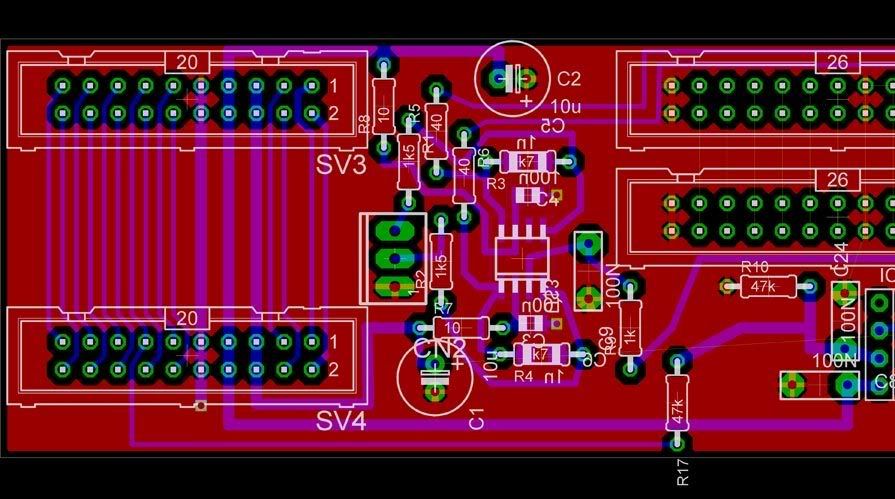
D4/5 are there to catch pathological input cases (someone sticks P48 up the thing for example), but I suppose it is arguable that given the 6db gain of the input stage we could drop them to 12V or so and run then in reverse breakdown the whole time which might improve their speed.
The intention is that the caps catch short surges and spikes and the zenner clamp deals with more major things.
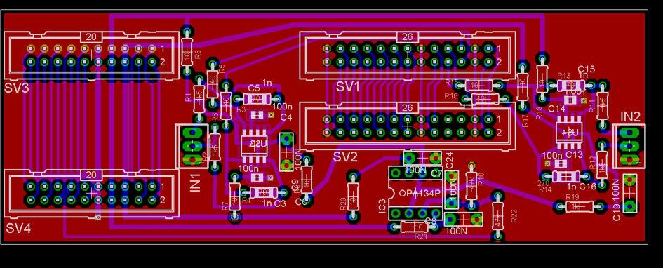
As to the two opamp instrumentation amp, you could do a three opamp one, but the key thing is that to get good noise performance you need to avoid large series input resistors because of the thermal noise (R7 & 8 are ok because they are in parallel with the source impedance which should be much lower then they are), a simple minded single opamp difference amp will be the dominant noise source if you are trying to get the differential input impedance higher then a few K.
Given the stated source characteristics (Highish Z, only a few metres of cable), I felt that the two opamp instrumentation amp would be sufficient, but it is a matter of taste.
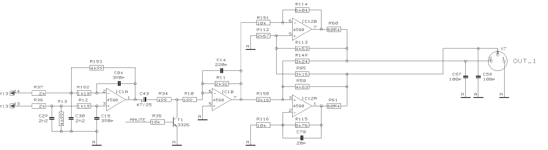
And yea, be careful with spice, it is a useful tool but the results always need sanity checking.
Regards, Dan.
The intention is that the caps catch short surges and spikes and the zenner clamp deals with more major things.
As to the two opamp instrumentation amp, you could do a three opamp one, but the key thing is that to get good noise performance you need to avoid large series input resistors because of the thermal noise (R7 & 8 are ok because they are in parallel with the source impedance which should be much lower then they are), a simple minded single opamp difference amp will be the dominant noise source if you are trying to get the differential input impedance higher then a few K.
Given the stated source characteristics (Highish Z, only a few metres of cable), I felt that the two opamp instrumentation amp would be sufficient, but it is a matter of taste.
And yea, be careful with spice, it is a useful tool but the results always need sanity checking.
Regards, Dan.
") It will aks to mak one more "floor" for 1U box but that's not a problem. ;D
It will aks to mak one more "floor" for 1U box but that's not a problem. ;D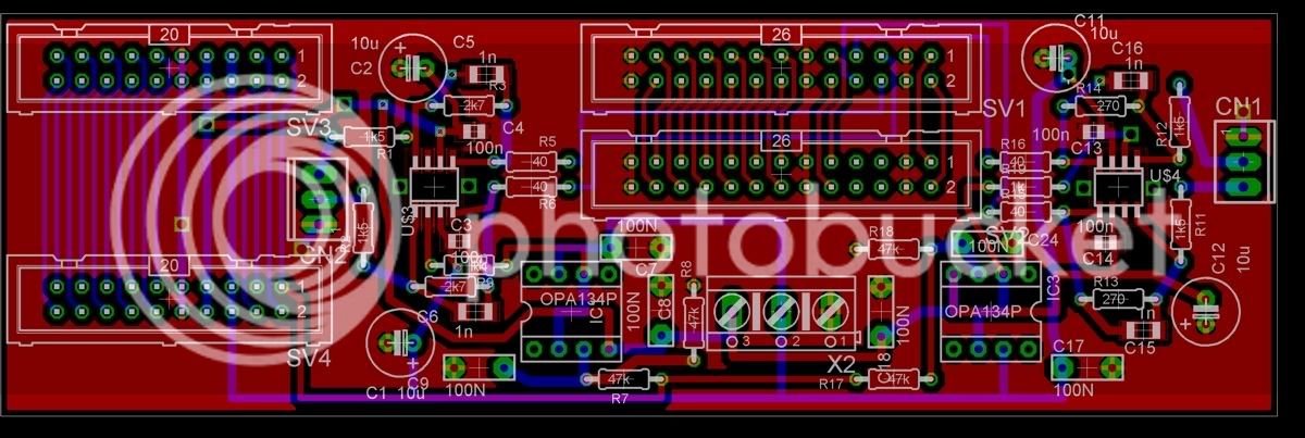


![Soldering Iron Kit, 120W LED Digital Advanced Solder Iron Soldering Gun kit, 110V Welding Tools, Smart Temperature Control [356℉-932℉], Extra 5pcs Tips, Auto Sleep, Temp Calibration, Orange](https://m.media-amazon.com/images/I/51sFKu9SdeL._SL500_.jpg)