IC Line Mixer - Bus Assign and Output Stage - seeking critique

GroupDIY Audio Forum

Help Support GroupDIY Audio Forum:

This site may earn a commission from merchant affiliate links, including eBay, Amazon, and others.

adastra

Active member
Joined
Oct 8, 2012
Messages
32
Howdy,
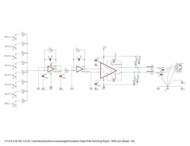
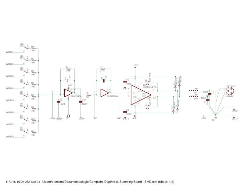
I'm a newbie at the design side of audio, but I'm attempting to build a simple utility mixer for a specific use.  Fidelity is not key here, this is essentially for routing band and crew talkbacks and such.  That said, I would like to learn and make the best circuit I can for a reasonable cost.  The schematic here is the bus switching (via relays) and output stage.  The output stage is made of 2 consecutive OPA134's configured for a 3dB loss each, then to a 1646 balanced line driver.  I've never really gone this deep into an audio design, so I'm looking for some feedback.  Feel free to tell me I'm completely lost, or if I'm lucky maybe I just have a few adjustments to make.  Any help is always much appreciated.

Notes
- most of the relay stuff I left off this schematic for simplicity, but its being driven by uC -> mcp23017 -> uln2803.
- The 10uF caps on the 1646 are BP, I just used that polarized symbol as it was the right size for the pcb.
- notation on the grounds is a little odd at the moment, but the idea was to take dirty, clean, and digital grounds to a star at the chassis

Thanks,
AdAstra
 

Attachments

  • 1646 Summing Board - SMD2.pdf
    35.8 KB · Views: 44
Using relays is inconsistent with modest sound quality and low cost. Look at CMOS transfer gate technology for lower cost ways to route medium fidelity signals.

JR
 
gyraf said:
..you will probably want to switch unused (muted) mix-resistors to ground...

Jakob E.

Got it, I guess this is the scheme with higher bus noise gain, but with such a low channel count I guess it won't be an issue.
 
JohnRoberts said:
Using relays is inconsistent with modest sound quality and low cost. Look at CMOS transfer gate technology for lower cost ways to route medium fidelity signals.

JR

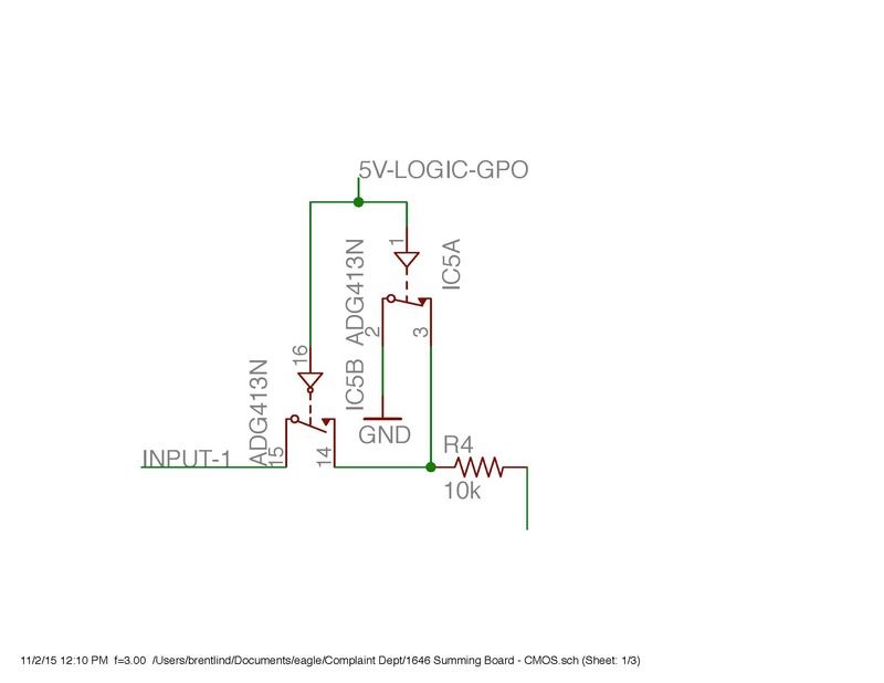
That would certainly save me a lot of board space and $.  Is this on the right track?
 
I was thinking even cheaper than those... those look pretty nice for higher voltage CMOS process, than the old CD4016/4066 I used back decades ago.

JR.
 
Am I missing supporting circuitry on the CMOS gates?  Any problem splitting the logic signal to 2 gate channels?  These packages don't end up saving me that much board space, but they do cut cost in about 1/2.  I suppose its just cost/benefit analysis at this point.
 
I'd rather put the switches before the resistors than after, ou still switch them to ground so they don't end flying around but you reduce the noise gain while doing so. The problem is you keep the load on the source instead of lowering it but it should be able to drive it anyway.

JS
 
adastra said:
a 1646 balanced line driver. 
I see you have put somme attention to the grounding, by grouping the RF protection caps with the reference ground and earth in the commonly called "star-ground" fashion.
I think for such a minimal design, grounding is not ultra-critical, but if you want to go the whole way, the 1616's decoupling caps should also be tightly grouped with this ground. The output current that flows through load is reflected in the decoupling caps and should therefore be discharged into the load's "ground". Indeed it's often very difficult to do but you should consider optimizing the length and width of the PCB track that joins them. As usual, the grounding should obey the famous motto "ground follows signal".
Now it seems the gain structure is not what you describe, since the 1st stage has 6dB attenuation.
 
abbey road d enfer said:
Now it seems the gain structure is not what you describe, since the 1st stage has 6dB attenuation.

Aha, I knew I'd do something silly.  If I set R1 & R2 to around 7K, that should change the ratio to 0.7 for a 3dB loss at each 134 stage, correct?  Then the balancing stage should put me back at 0dB right?

Your grounding notes are very helpful, I'll be sure to reference them as I get deeper into the layout. 
 
joaquins said:
I'd rather put the switches before the resistors than after, ou still switch them to ground so they don't end flying around but you reduce the noise gain while doing so. The problem is you keep the load on the source instead of lowering it but it should be able to drive it anyway.

JS
Sorry I'm confused, don't I already have the switches before the bus resistors?
 
adastra said:
joaquins said:
I'd rather put the switches before the resistors than after, ou still switch them to ground so they don't end flying around but you reduce the noise gain while doing so. The problem is you keep the load on the source instead of lowering it but it should be able to drive it anyway.

JS
Sorry I'm confused, don't I already have the switches before the bus resistors?

  Sorry, the other way around, I was the confused... Few days without sleep (cheek-tooth)

  If you put the switches after the resistor the noise gain is the number of used channels plus one, if you put it before is the total numbers of channels plus one all the time. Also it's quite good to have the switches as close to the bus conductor as possible to avoid having the open wire all the time as well as have the bus conductor terminated at both ends, one usually with the summing amp, the other with the first channel ideally, so at the first channel having the switch before and all the rest after the resistor. Avoid antenas would be the idea.
  Doing a small 6 channel mixer is probably not a big deal all this. Working on a 32 big sized desk it's quite a big deal, having NG of 33 all the time Vs 4 when only using 3 channels in a bus is quite a difference and having a 1m unterminated antena also is a big deal, that with the capacitance of the conductor going directly to the non inverting input of the OA could ruin your day.

JS
 

Latest posts

Back
Top