Gentlemen,
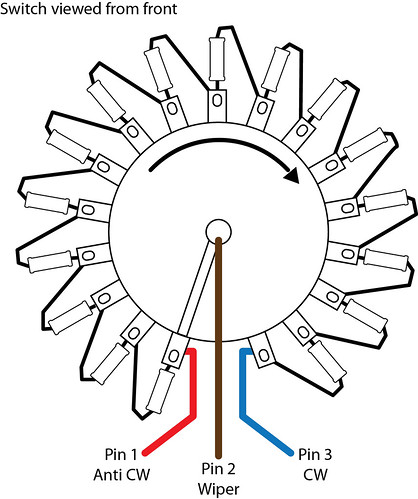
I have created a diagram for my stepped switches (I need these visual aids) and I'm wondering if you can give it a look and make sure that I'm going to do this right.
The switch is viewed from the front (shaft) side and I have labeled the connections as Pin 1 Anti CW...etc.

So if looking at my diagram, if I were using this switch as the Hi Boost Lin pot (switch) then Pin1 would be connected to T1 of the High PCB.
Pin 2 would be connected to T2 of the High PCB. Pin 3 would be connected to Pin3 of the Hi Cut switch, correct?
Conversely, if this were the Lo Boost Log pot (switch), Pin 1 would be connected to T1 of the Lo PCB while Pin 2 would be jumpered to Pin 3 and Pin 3 would be connected to T2 of the Lo PCB as well as Pin 1 of the Hi Cut pot (switch).
Does this sound right? Basically I'm trying to make sure I'm connecting the wires correctly to the switch (pot).
Thanks
Dave








![Soldering Iron Kit, 120W LED Digital Advanced Solder Iron Soldering Gun kit, 110V Welding Tools, Smart Temperature Control [356℉-932℉], Extra 5pcs Tips, Auto Sleep, Temp Calibration, Orange](https://m.media-amazon.com/images/I/51sFKu9SdeL._SL500_.jpg)


