Zener Diode vs Linear Voltage Regulators?

GroupDIY Audio Forum

Help Support GroupDIY Audio Forum:

This site may earn a commission from merchant affiliate links, including eBay, Amazon, and others.

carboncomp

Active member
Joined
Feb 22, 2022
Messages
41
Location
England
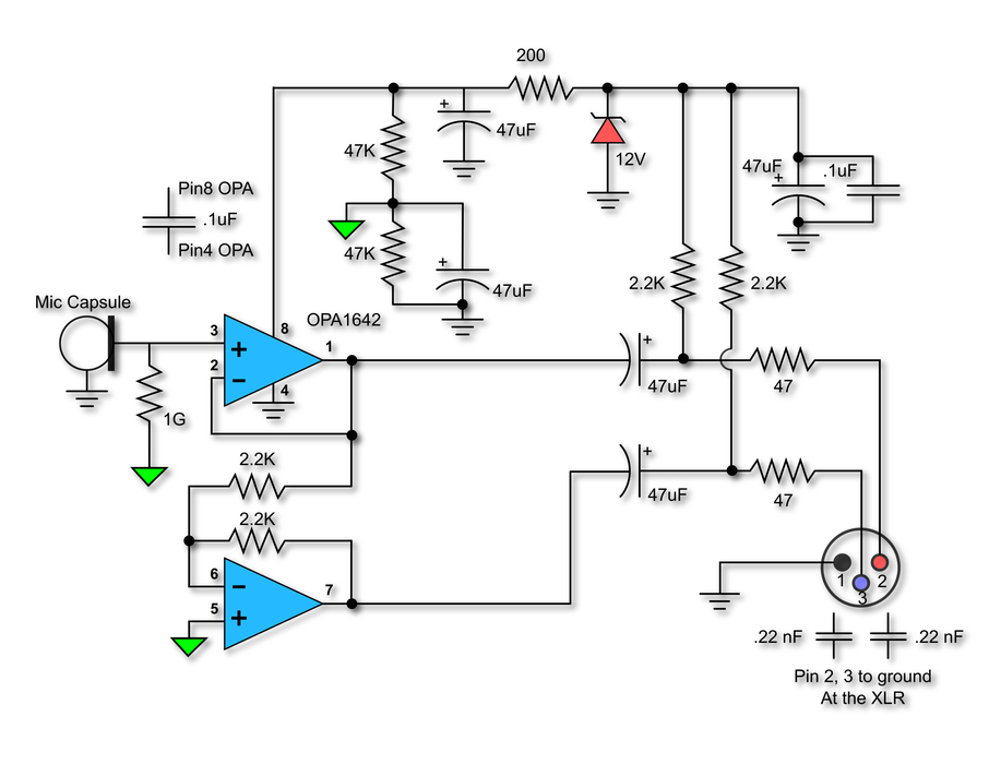
Hi, just wondered if someone could explain to me why this circuit uses a Zener diode for the 12V rail over an LVR?

ci7HMm2.png


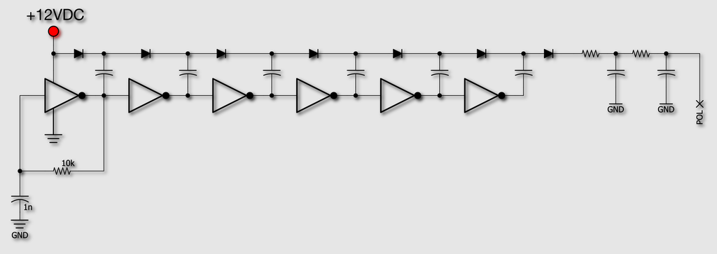
More interested in the variant that uses that 12V supply to get 80v out of a Hex inverter to use a LDC:

JUiPBDG.png


Sorry first LDC build so asking a lot of noob questions!
 
It's taking the phantom voltage (which should be clean DC) and clamping at 12V. Not much need for a regulator here.
Thank you. if I wanted a wider range of bias voltages for the LDC, could I use a higher value diode say 14V and then put a resistor and a trim pot as a voltage divider to change the now 14V going into the Hex inverter?
 
as a warning, some usb interfaces don't have clean phantom power. I have an audient id14 mk2 that works fine with most mics but outputs a bizarre quiet screeching when using a cheaper schoeps style mic
 
There is no actual requirement to regulate the op-amp supply for this configuration.
The 'half rail' used to create the artificial 'ground' for the dual DC supply the op amp requires (2 x 47K resistors in this case) will automatically adjust to suit the DC derived from the phantom power.
(You would probably use a higher value than 2k2 for the feed resistors, when no zener is fitted).

In the case of the Hex inverter multiplier, a regulated supply will allow the output voltage to be calculated more precisely.
Using a zener for this task is more useful.

I only used a regulated supply for the multiplier on the circuitry I used for my own version of an OPA164* impedance converter.
Using a 12V zener allowed for the easy selection of a polarisation output voltage within the range 60V - 80V.
(Some notes here: www.opic.jp137.com )

The application of a Hex inverter for this task dates back to at least 1983, when Rory Holmes published his ETI magazine article on the subject.
(You can find a copy of that article HERE )
 
Last edited:
There is no actual requirement to regulate the op-amp supply for this configuration.
The 'half rail' used to create the artificial 'ground' for the dual DC supply the op amp requires (2 x 47K resistors in this case) will automatically adjust to suit the DC derived from the phantom power.
(You would probably use a higher value than 2k2 for the feed resistors, when no zener is fitted).

In the case of the Hex inverter multiplier, a regulated supply will allow the output voltage to be calculated more precisely.
Using a zener for this task is more useful.

I only used a regulated supply for the multiplier on the circuitry I used for my own version of an OPA164* impedance converter.
Using a 12V zener allowed for the easy selection of a polarisation output voltage within the range 60V - 80V.
(Some notes here: www.opic.jp137.com )

The application of a Hex inverter for this task dates back to at least 1983, when Rory Holmes published his ETI magazine article on the subject.
(You can find a copy of that article HERE )
Thank you so very much.

My goal is to have an LDC with each side of the capsule broken out to its own 3 PIN XLR so I can get a whole bunch of patterns using the mixer and Inverts the Polarity.

So, looking at your design I could just use a 5 pin XLR, and two copies of the same circuit on one PCB?

So, I could just use 2 OPIC.41 circuits on the same PCB, and have a second PCB with the OPIC.VM on it, and switch out R5 for a 3K3 Trimpot, and I would essentially have everything I need for builds using LDC's, with an adjustable bias for the charge on the LDC that can be broken out to form a 5 pin to two 3 XLR pin cables (assume a common ground is not going to be an issue?).

Any pitfall with taking that approach?
I used a very similar construction concept for the 'Mid/Side' version of the project I posted in the notes I linked to above.

(See this PDF for more details : http://www.jp137.com/lts/OPIC.M.S.pdf )

You would probably need to fit the op-amp stripboard on the top side of the frame, with the VM stripboard on the other side, with all the components facing 'outwards' (As I have done for the LDC version of the project).

For the LDC version I has to ensure that the components were mounted as near to the centre of the stripboard as possible, so that when mounted on the top side of the frame there was sufficient clearance between the stripboard components and the body sleeve.
For the Mid/Side version I used electrets, so the clearance issue was not a problem because the stripboard could be mounted underneath the frame with the components facing 'inwards' as it were....
So you might need to check the 'component to sleeve' clearances, if you use the layout I've used for the dual version, and you need to fit the stripboards with components facing 'outwards'?

One other thing is that - unlike Jules' Alice OPA - I've gone for a single sided audio output, with the second side 'passively balanced' to ground.
That has three advantages..
• It has a marginally lower noise floor than the differential version (the resistors in the inverting op-amp will add noise, as well as gain.)
• It requires fewer components per output - and you're looking for 2 separate outputs here.
• Each output only draws half the current that a differential output would require.
First, thank you so much for all that info, really is going above and beyond and it is sincerely appreciated.

Would you mind terribly if I asked a couple of very beginner-level questions, as you seem to already achieve the layout for exactly what I would like to build?

Rather than stripboard, I was thinking of going with PCBs to pad out a PCB order for some other projects.
(first, would that be ok with you, this is just a DIY project and not going to be selling any of the PCBs, but feel it's the right thing to at the very least ask the creator).

I happened to notice the Jules' Alice OPA schematic seems to be using what I believe are Net Ties? on the grounds of each circuit that google tells me is used to separate analog/power/digital. Is this something the stripboard version inherently does by the layout out itself, and if moving to a PCB layout for the 'Mid/Side' version of the project would I have to keep anything in mind, such as avoiding just using a ground pour, and rout the ground traces separately only meeting at the common ground on the XLR?

Once again thank you for your help and having put such an easy to follow gateway to DIY mics out there for people like me!
 

Attachments

  • l9zjvrnxe1k81.png
    l9zjvrnxe1k81.png
    103.8 KB
You are most welcome to use any of my circuit ideas if they are of any help ...
Like Jules - who came up with his idea of using these OPA164* op-amps as impedance converters for hobby mics - I like to see DIY hobby mic ideas shared and developed by other mic builders.

The idea of using 'star' earths to minimise eddy currents is well documented, and the separation of digital and analogue grounds are often best served with that idea.
In the case of my stripboard layouts I have endeavoured to adopt that technique from my ground connection (XLR pin 4 in this case), although in this application it's not as critical a consideration as it can be on other occasions.
Another approach is the idea of a double sided ground plane layout where - in essence - everything is ground until required not to be!
That was the approach taken by Khron who did the PCB layout for my RF bias mic project (see THIS PAGE for that PCB layout detail)

I notice on your schematic that you have still included 2 x dual OPA1642, to provide 2 differential outputs rather than going single sided ?
You have also duplicated the zener regulator circuitry, which is probably not really necessary.

You might need to check out the current drawn by the circuitry on your schematic? Each OPA1642 draws around 4 mA, plus the zener currents.
Add to that the VM (Voltage Multiplier) circuit current, and that's going to get pretty close to the maximum recommended for 48v phantom power usage (10mA).... Maybe even slightly above it?
You might like to look again at reducing current drain by considering a single op-amp for each channel..... and only regulating the VM supply?

I would suggest maybe trying out a stripboard prototype, before committing your design to a PCB layout?
I find it's usually easier (and cheaper) to revise stripboards than it is PCBs!

One final point. You'll notice from my layout that I keep the connection between the 1G resistor and the capsule 'off board' as it were.
This point is extremely high impedance, and it's not a bad idea to keep it away form any flux or dirt that might be present, if that connection is soldered directly to the stripboard (or PCB!) . That can make things noisy - especially in the longer term.
 
Last edited:
I notice on your schematic that you have still included 2 x dual OPA1642, to provide 2 differential outputs rather than going single sided ?
You have also duplicated the zener regulator circuitry, which is probably not really necessary.

You might need to check out the current drawn by the circuitry on your schematic? Each OPA1642 draws around 4 mA, plus the zener currents.
Add to that the VM (Voltage Multiplier) circuit current, and that's going to get pretty close to the maximum recommended for 48v phantom power usage (10mA).... Maybe even slightly above it?
You might like to look again at reducing current drain by considering a single op-amp for each channel..... and only regulating the VM supply?
Oh, that's not my layout, that's from Jules instructable True Condenser OPA Mics was planning on starting a copy of yours tomorrow. I think his intention was to make a PCB kit that could be used for both single and double applications so has just cut and pasted the two single-board schematics together with the idea of only populating what is needed...though it seems his premade PCBs are fully populated, not quite sure now you mention it?

Would it be too much to ask if I post my schismatic in here tomorrow you would be good enough to give it a look over to see if I made any mistakes?

Again, thank you, you have been a wealth of information!

Oh and terribly sorry, but the link here seems to be missing:
Another approach is the idea of a double sided ground plane layout where - in essence - everything is ground until required not to be!
That was the approach taken by Khron who did the PCB layout for my RF bias mic project (see THIS PAGE for that PCB layout detail)
 
I can certainly cast my eye over your schematic and see if I can spot anything strange....

Sorry about the broken link - try THIS
 
I can certainly cast my eye over your schematic and see if I can spot anything strange....

Sorry about the broken link - try THIS
Thank you, will give that a read!

Here is what I have so far, so just to clarify what I want is to be able to take both sides of an LDC like the TSC-2, have both sides independently mixed and or phase switched all running off the phantom power, and break the two mic channels out from a 5 pin XLR to two 3 pin XLR's for the mixer.

But, think I have confused myself with the section wired to the wiring into the LDC as your circuit was meant for two electret microphones, and maybe I should not be doing this at 3AM? 😀

Test.png
 
There are a few things that need addressing:

• You've forgotten to include the 10nF oscillator capacitor between pin 1 and ground of the 40106 (C1 on my schematic)

• R17 on your schematic needs to be 1M (or higher - value not critical above that value) not 470R

• R15 and R16 each need to be 27k rather than 470R.

• RV1 probably needs to be 5k rather than 3k3 - 5k pots are easier to source - ( Bourns 3386 for example )

• Pin1 of each capsule needs to go to the output of the voltage multiplier, and not to the 'half rail' . (As you have noted, that is for the FETless electret option)
(I would suggest that you take the common backplate connection to the output of the multiplier, and the 2 individual centre terminations to each of the 1G resistors. The other end of both of those resistors should go to half rail, as you have already drawn).

• R9 (470R) doesn't actually need to be there at all. I had included it to provide a test point on my original prototype, and its removal got missed!

• You've drawn the 22nF RF decoupling caps as if they are to be fitted directly to the XLR pins themselves. I know this is often recommended, but it would be very fiddly to fit 4 capacitors onto a single 5 pin XLR. I think you'll find adding them to the stripboard/PCB itself - as close to the XLR termination points as possible - will probably work just as well, and will be much simpler to fit!

• If you are keen to maximise the voltage multiplier output range, you might like to fit D3 as a15v Zener, rather than 12v?
Do remember though that the higher the voltage, the more likelihood of the capsule collapsing.... And the difference in sensitivity between - say - 70V and 80V is only likely to be 1 dB or so.
The TSC capsules you've suggested seem to be pretty 'standard' Chinese K.67 type centre terminated capsules, so should be OK with 80V.
Try adjusting for values between 60V and 80V and see how much difference you notice....

Thank you for taking the time to look that over and pointing out my mistakes. I think I have addressed them all (but may very well have missed something) Have I done the 1G resistors right?

test 2.png
 
Thank you for taking the time to look that over and pointing out my mistakes. I think I have addressed them all (but may very well have missed something) Have I done the 1G resistors right?

View attachment 91335
Looks fine -- although you do need to remember that if you do decide to use a 15v Zener rather than 12V then with the rheostat set to its minimum value the maximum output voltage will be around 100V .
Right on the limit of the capacitor ratings, and maybe too much for the capsule? ....
 
Looks fine -- although you do need to remember that if you do decide to use a 15v Zener rather than 12V then with the rheostat set to its minimum value the maximum output voltage will be around 100V .
Right on the limit of the capacitor ratings, and maybe too much for the capsule? ....
Think it would be safer to go 13V Zener Just to bring that voltage down a little, but still be able to hit 80v and keep the caps (and capsule for that matter within spec?) What would that be, 13x7=91V in theory, so just over 80V in reality?
 
A zener or other shunt regulator can be used as part of a safely system for a phantom powered microphone.
Say the phantom power supply fails and goes over 52VDC?
A properly designed microphone circuit could save the microphone from damage.
 

Latest posts

Back
Top