moamps
Well-known member
What's real purpose of using ground planes on LF circuits except saving the etching chemicals?


I don't think I'm mixing anything. Grounding is a one and single issue.squarewave said:I think we're starting to mix up grounding issue principles (which is easy to do).
Isn't it what grounding is about?My understanding is, and correct me if I'm wrong, that the "ground follows signal" rule has to do with EMI and magnetic coupling of noise into other parts of the circuit.
How is it a separate issue? We are debating about how to connect different "grounds" in such a way that noise performance is optimized.Then you have parasitic resistance / inductance which is a separate issue
Here you are again with your notion of a dirty ground that should not be connected because its "dirt" will be amplified by the high-gain circuit. What would cause the output "ground" to be dirty vs. the input "ground"? If currents are well balanced and referenced to a single point in the output "ground", why would it be dirty?However, I think there's a 3rd issue (although it does have to do with parasitics) which is that, because the circuit in question is high gain, any noise on the input is going to be amplified and, if the output ground is connected to the input ground,
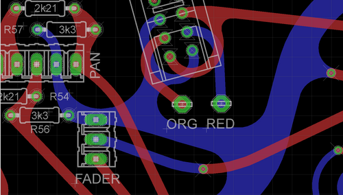
You should really check the pitch of the parts you are using.Icegoldnixon said:Another layout with minor updates.
A) When well designed, i.e. not allowing output currents to circulate in sensitive nodes, a ground pour has lower resistance (and inductance) than a basic ground trace.moamps said:What's real purpose of using ground planes on LF circuits except saving the etching chemicals?
All this can be done without ground planes.abbey road d enfer said:A) When well designed, i.e. not allowing output currents to circulate in sensitive nodes, a ground pour has lower resistance (and inductance) than a basic ground trace.
B) It acts as an electrostatic shield that allows reducing unwanted capacitive coupling between nodes.
Do you think there is no benefit in decreasing the impedance of the reference node? I do. What do you suggest? Adding copper wire?moamps said:All this can be done without ground planes.
The capacitance of a 0.3mm trace respective to a ground plane is about 1pF/inch (4pF/dm). Not an issue, unless dealing with extremely high impedance nodes. I wouldn't use a ground plane with the gate connection of an FET in condenser microphone, but apart from that, a few pF capacitance is not significant.B) with ground planes you have capacitive coupling to the ground, forming LF filters.
moamps said:What's real purpose of using ground planes on LF circuits except saving the etching chemicals?
There is noise on the input. Just from Johnson noise or whatever. That is going to be amplified 100x because the circuit is high gain and then some of that noise is going to leak back into the input and be amplified again resulting in overall a slightly higher noise floor.abbey road d enfer said:Here you are again with your notion of a dirty ground that should not be connected because its "dirt" will be amplified by the high-gain circuit. What would cause the output "ground" to be dirty vs. the input "ground"? If currents are well balanced and referenced to a single point in the output "ground", why would it be dirty?
That is true.squarewave said:There is noise on the input. Just from Johnson noise or whatever. That is going to be amplified 100x because the circuit is high gain
Why would it be so? Adequate design makes sure this does not happen.and then some of that noise is going to leak back into the input
No. DGND stands for "digital ground"; calling it dirty ground is an abuse.I never said anything was "dirty". I can only guess you are getting that from the name "DGND" that I use to mean a ground for anything that is not relatively quiet.
That's exactly what you say in the former sentence. You contradict yourself. Again, "digital or relay stuff" is dirty only if the currents are not properly returned and they are allowed to flow and develop a voltage that may possibly be amplified. That is the first thing that needs to be addressed.So if there IS something "dirty" like digital or relay stuff it sound use DGND. I did not mean to say something was "dirty".
True. It depends on the load. But the circuit as shown could be any load. If it's a 600R load there will be amplified noise on the ground. If it's a 5K pot feeding another stage, then it would not be a problem.abbey road d enfer said:Why would it be so? Adequate design makes sure this does not happen.
It does not depend on the load; it depends on how the load current is returned to ground. It this point is well chosen, whatever the current, there would be no interference with the input.squarewave said:True. It depends on the load. But the circuit as shown could be any load. If it's a 600R load there will be amplified noise on the ground. If it's a 5K pot feeding another stage, then it would not be a problem.
")
In a lot designs I saw here, using GP wasn't resulting in decreasing this impedance. Ground planes are not a universal cure in LF circuits where impedances are not 50 or 75 ohms.abbey road d enfer said:Do you think there is no benefit in decreasing the impedance of the reference node? I do. What do you suggest? Adding copper wire?
The capacitance of a 0.3mm trace respective to a ground plane is about 1pF/inch (4pF/dm). Not an issue, unless dealing with extremely high impedance nodes. I wouldn't use a ground plane with the gate connection of an FET in condenser microphone, but apart from that, a few pF capacitance is not significant.
Well I would do some tests but all of my electronics stuff is tucked away right now since I'm working on work right now (or at least I'm supposed to be). But you have me wondering. I'm not an EE so I rely heavily on modelling and comparative measurements. I would swear that I have seen measurable differences using a separate ground for high gain inputs but I don't have empirical data and plots and such and I don't recall the exact the circumstances. If the circuit is just a simple stand alone mic pre with nothing else going on and the planets are aligned properly, then maybe it's not a problem (I never did say it definitely would be). At the noise levels we're talking about (-127-ish dB) it can be difficult to measure differences reliably. There have been many instances where I re-dress some wires or fiddle with a test cable and I get a slightly different result. My projects can be pretty elaborate with lots of relays, leds and digital all packed together so I decided long ago to use 3 grounds that get progressively quieter (smaller / lower freq. currents) and I would swear that if I use the quietest ground for just the mic in (what we have been referring to as "signal ground" or SGND in this discussion) I get better noise results.abbey road d enfer said:It does not depend on the load; it depends on how the load current is returned to ground. It this point is well chosen, whatever the current, there would be no interference with the input.
At audio frequencies, the larger the traces, the lower the resistance (inductance is negligible).moamps said:In a lot designs I saw here, using GP wasn't resulting in decreasing this impedance.
Ground planes are not supposed to be a cure, they are part of design in RF applications. In audio, they are convenient for the reasons I exposed earlier.Ground planes are not a universal cure in LF circuits where impedances are not 50 or 75 ohms.
Distance between signal traces and copper pour is adjustable in all PCB softwares. I also use 0.3mm clearance. If I ever found that it resulted in too high a capacitance, I would increase clearance, but it just never happened.This capacitance depends of the thickness of the board, but also the bigger problem are too small distances of the GP to the traces on the same layer.
0.3mm (12 thou) is a very common standard for low-level signal traces; not too long ago, if you wanted smaller traces, you had to pay extra. Now PCB fabs commonly do 0.1mm (4 thou), but I haven't changed my habits.Why you choose 0,3mm trace for your math?
0.3mm (12 thou) is a very common standard for low-level signal traces; not too long ago, if you wanted smaller traces, you had to pay extra. Now PCB fabs commonly do 0.1mm (4 thou), but I haven't changed my habits.
Ground traces benefit of being wider since it minimizes longitudinal noise. Power traces need be sized according to the current they carry.boji said:What are the pros/cons to using trace widths much larger for low level signal?
Remember how PCB artwork was produced then, using transfers and adhesive tape on a transparent film. The thinnest tape was about 0.5mm (20 thou) and that ended up being the actual resolution, unless you did scale 2x, which required an additional photographic step. Actually, at the time I didn't go below 0.8mm, except for logic.I've been using 2oz , 1.27mm for the 70's inspired stuff. Were larger trace widths only due to fabrication limitations of the day?
Icegoldnixon said:Wow! Thank you, pedantic is what I crave. ... Happy Memorial Day!
Good luck with your endevours Enter your email address to join:
