You are using an out of date browser. It may not display this or other websites correctly.
You should upgrade or use an alternative browser.
You should upgrade or use an alternative browser.
[BUILD] CAPI LC53A~500 Series~Love Child EQ Kit~Official Support Thread
- Thread starter jsteiger
- Start date
Help Support GroupDIY Audio Forum:
This site may earn a commission from merchant affiliate
links, including eBay, Amazon, and others.
stringmike
Member
- Joined
- Nov 13, 2014
- Messages
- 18
I just finished the build of 2 lc53's, but none of them are passing audio. Regardless of the bypass button is in or out. The calibration went well, so I guess the first place to start would be the second op amp? Any other places to look?
stringmike
Member
- Joined
- Nov 13, 2014
- Messages
- 18
OK, started on the first and switched the DOA's to ones that I knew 100% were working, but still no luck. Before I went signal hunting, I trimmed the DTO5s and the voltage followers nicely on the back, since I didn't have a good trimming tool when I made those. I covered the back with insulating tape as well, and now, the unit passes audio, so there must have been a short somewhere here. But the audio distorts. When I engage the HPF, the audio gets even louder, and distorts even more. The other filters seem to be working properly (apart from the distortion). The amount of distortion depends on the input level of the material.
stringmike
Member
- Joined
- Nov 13, 2014
- Messages
- 18
BTW, the audio level matches very well both in bypass and in, so no issues here.
stringmike
Member
- Joined
- Nov 13, 2014
- Messages
- 18
Update: I worked on the second one, and after trimming the DTOs and the DFs, it worked! So I swapped first the DTOs from the working unit and then the DFs, and the last DF (A1) turned out to be bad. I checked the components, everything working here. But there was one soldering, that looked a little odd. So I resoldered, and voila! Both units alive and kicking!!
So as Jeff points out: It's imperative
to point out that each and every single lead at the bottom of this PCB must be trimmed as close as possible to the PCB!!!
So as Jeff points out: It's imperative
to point out that each and every single lead at the bottom of this PCB must be trimmed as close as possible to the PCB!!!
gar381
Well-known member
stringmike said:since I didn't have a good trimming tool when I made those.
These guys are your best friend when building LC53s
http://www.all-spec.com/products/CHP-170.html
Take it from a guy that has built 8
GARY
A small update. The power supply seemed to be at least part of the problem. I now have a consistent reading for 2 out of 3 units and I could do the CMM test with those units.
The third one still gives me trouble though. The trimmer doesn't seem to have any influence and I'm stuck between 40 and 240 mV at the negative side of C2.
I've swapped the opamp.
I've desoldered the big caps and tested them.
I've desoldered the diodes and tested them.
I've desoldered the big resistor and tested it.
I've desoldered the trimmer and tested it.
They all seem fine.
As said this is one out of three units that cosmetically look the same. The soldering looks fine and I see no physical damage anywhere.
Does somebody have an idea where else to look? I hope I'm not overlooking something stupid.
Any help is greatly appreciated! Thank you very much.
Oooops question....
This is a picture of the main PCB underside of C7; you can see I got too aggressive (slipped) with my cutters and snipped the underside pad right off. Dang. I seemed to have flowed enough solder that the damaged pad leg does make continuity with several spots on the PCB that I assume it is supposed to (it seems to connect to many grounds - pin 13 ground on the rack mate pins, the bottom right corner ground on the PCB mount, + side of C8, - side of C9,etc) . Should I just move on thanking my lucky stars that the connection seems good?
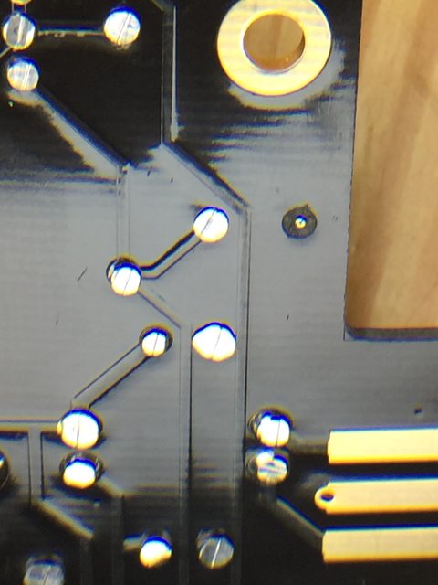
This is a picture of the main PCB underside of C7; you can see I got too aggressive (slipped) with my cutters and snipped the underside pad right off. Dang. I seemed to have flowed enough solder that the damaged pad leg does make continuity with several spots on the PCB that I assume it is supposed to (it seems to connect to many grounds - pin 13 ground on the rack mate pins, the bottom right corner ground on the PCB mount, + side of C8, - side of C9,etc) . Should I just move on thanking my lucky stars that the connection seems good?

That is the ground connection for that cap. Since the ground plane is on the other side of the board and the holes are plated thru, it sounds like you have enough solder in the barrel of the hole. To be safe, you could solder a short jumper wire from that lead over to the ground pad of C8. That is the hole that has no visible trace running to it. You could also just heat up that nub of a lead and add a little more solder to what is showing. That is what I would do. 
jsteiger said:That is the ground connection for that cap. Since the ground plane is on the other side of the board and the holes are plated thru, it sounds like you have enough solder in the barrel of the hole. To be safe, you could solder a short jumper wire from that lead over to the ground pad of C8. That is the hole that has no visible trace running to it. You could also just heat up that nub of a lead and add a little more solder to what is showing. That is what I would do.
Thank you Jeff! About to do CMRR later today - voltages on pins and transformer wiring holes are good.
Hi all! I built an LC53. While doing final testing, both the HPF and LPF work and both the HI and LO bands work at all frequencies in shelf/bell.
However, the midrange boost/cut gives me nothing. All components are in their correct places/polarities with known working GAR-2520s in place and I don't see any bridged or cold solder joints.
Anyone have any ideas as to what the issue is? Thanks!
jt burke
However, the midrange boost/cut gives me nothing. All components are in their correct places/polarities with known working GAR-2520s in place and I don't see any bridged or cold solder joints.
Anyone have any ideas as to what the issue is? Thanks!
jt burke
Musepro said:Hi all! I built an LC53. While doing final testing, both the HPF and LPF work and both the HI and LO bands work at all frequencies in shelf/bell.
However, the midrange boost/cut gives me nothing. All components are in their correct places/polarities with known working GAR-2520s in place and I don't see any bridged or cold solder joints.
Anyone have any ideas as to what the issue is? Thanks!
jt burke
I went ahead and reflowed the solder joints, swapped the DT05 and DF2 positions and tried another pair of 2520s from two of my VP28s, but I still have no midrange boost/cut, even though every other function works perfectly and the unit calibrated well and sounds good. Any thoughts?
jt burke
Attachments
JT, sorry for the delay. I was away in Nashville for a week and have been hammered with store orders since my return.
With the boards plugged in and assembled to each other, make sure you have continuity between the switch wiper of the CB-PCB's SW4 and the LC-EP PCB's SW3 wiper. If not, look at the center pin of J2's header/socket. Its J2 on each PCB.
If that is all good, I would look to make sure the common pin of L3 is getting to ground thru R11 when the EQ circuit is engaged.
If you have a good way to desolder, I would next remove L3 and measure DCR from the common pin to any and all of the other used pins of the inductor. I do check each and every inductor when I receive the batches to make sure none are open circuit.
Jeff,
I have solid continuity between the wipers (C1) of SW3 and SW4. All 3 pins of J2 are solid between the boards as well. Common pin of L3 to ground is solid, before and after the 2.1K R11 resistor with EQ engaged. I removed L3 and, looking at L3’s bottom with the common at top left going down, I get DCRs of 24.5, 31.7 and 45.8; then NC, NC, 62.9 and 63 down the other side. I did not attempt to measure inductance.
What do you think? Thanks a lot!
Attachments
Hmm, well that all checks out. If you have DCR, the inductance will be fine and nothing looks open there.
My next thought is that the stop pins are in the wrong spot on the freq select Grayhill on the LC-EP PCB.
My next thought is that the stop pins are in the wrong spot on the freq select Grayhill on the LC-EP PCB.
jsteiger said:Hmm, well that all checks out. If you have DCR, the inductance will be fine and nothing looks open there.
My next thought is that the stop pins are in the wrong spot on the freq select Grayhill on the LC-EP PCB.
Good grief! I removed the stop pins and spun the switch around, all 5 frequencies work perfectly! I obviously had the switch in the wrong position when I installed the pins at noon and 5. Thanks for helping Jeff! Happy it was only a minor, simple fix!
I do have a question about the stop pin placement; On the HI and LO bands, which have been working perfectly from the start, with the pins at noon and 5 on the 2-pole SW1/4, I get one click below and one click above the frequency range (7 positions). I assumed this was to facilitate single band bypass. However, with the pins in the same noon-5 holes of the 1-pole SW3 mid band switch, it lines up perfectly with only one click per frequency (5 positions). Is this correct? Thanks!
All switches should only travel to what is designated on the faceplate, not one position further each way. I would imagine those were also moved before the pins went in? Hence 7 positions instead of 5. 12-7=5 so those wipers are also between the wrong sides of the stops pins.
jsteiger said:All switches should only travel to what is designated on the faceplate, not one position further each way. I would imagine those were also moved before the pins went in? Hence 7 positions instead of 5. 12-7=5 so those wipers are also between the wrong sides of the stops pins.
Got it. Not sure why I was confused about the FREQ switch positions before I installed the pins, but it's clear to me now. Everything is perfect now. Thanks!
hello all!
just finished with building 2 units. the first works, the second one too but has around 6 or 7dB less output. this is also the case when the unit is in bypass. i've already interchanged all DOA and DVF from both units but it's still the same. in the second unit there's no L1 4H inductor installed yet, but according to jeff this shouldn't be the problem.
can someone plz help me troubleshooting from here?
thx in advance,
Georg
Georg, the inductor won't be the cause since it not being installed is no different than what happens when the EQ is not "ON". The LCR series component strings are lifted from ground when not ON.Tschem said:hello all!
just finished with building 2 units. the first works, the second one too but has around 6 or 7dB less output. this is also the case when the unit is in bypass. i've already interchanged all DOA and DVF from both units but it's still the same. in the second unit there's no L1 4H inductor installed yet, but according to jeff this shouldn't be the problem.
can someone plz help me troubleshooting from here?
thx in advance,
Georg
Since you have already swapped around all of your opamps and followers, it must be a couple of accidentally swapped resistors. Near the beginning of this thread, I posted a procedure to check audio levels at certain points throughout the audio path. Locate that post and follow those instructions. There is a PDF posted with test points to take ACV readings while injecting a sine wave. This will help narrow down the stage where the problem starts.
Similar threads
- Replies
- 6
- Views
- 773
- Replies
- 1
- Views
- 1K
- Replies
- 3
- Views
- 958
- Replies
- 80
- Views
- 23K





![Soldering Iron Kit, 120W LED Digital Advanced Solder Iron Soldering Gun kit, 110V Welding Tools, Smart Temperature Control [356℉-932℉], Extra 5pcs Tips, Auto Sleep, Temp Calibration, Orange](https://m.media-amazon.com/images/I/51sFKu9SdeL._SL500_.jpg)
