Comments on my first PCB layout please

GroupDIY Audio Forum

Help Support GroupDIY Audio Forum:

This site may earn a commission from merchant affiliate links, including eBay, Amazon, and others.
Last time I did this at home, I printed the positive image onto clear transparency film (made for being heated in a laser printer) with a laser printer set to maximum black.  I printed it out twice onto two films actually.  I then stacked them on each other and placed on the sensitized PCB, exposed for however long was recommended, and then etched.  They came out very clean, despite my reservations about bleed through of the light around the edges (which didn't end up happening).

But to be honest, you can get real PCB's made for less than $1 per sq. in., with real solder masks and silkscreens and fully plated through-holes.  The chemicals alone cost more than that!
 
Matador said:
to be honest, you can get real PCB's made for less than $1 per sq. in., with real solder masks and silkscreens and fully plated through-holes.  The chemicals alone cost more than that!

Totally...but the waiting sucks, haha.
 
Ptownkid said:
Let me check, i should have some around that i won't use now that I have a cnc. Also, you can get pulsar transfer film from rp-electronics.com in canada.

Cool! I have looked at the photo transfer stuff, but doesn't the PCB need to be pre sensitized? Might have to go down to RP. I live about 30 minutes away from there.

Yeah, getting PCB's made professionally is the easiest. No mess, soldermask, silkscreen, but then what am I going to do with the big bottle of ferric chloride I just bought? Plus, I think there will be a sense of satisfaction that comes along with going DIY all the way.
 
Ptownkid said:
They have an iron on transfer film...if you can, return the ferric chloride and buy some ammonium persulfate instead

Will check that out.

I bought the ferric chloride from Main electronics here in Vancouver. No refunds, no exchanges, no exceptions. I actually stood in the store for 10 minutes or so trying to decide between the 2. Oh well.
 
Insomniaclown said:
Plus, I think there will be a sense of satisfaction that comes along with going DIY all the way.

This is true.  I was like a kid in a candy store the first time I swirled around the FeCl solution and saw my circuit appear as if by magic. ;)

Make sure you lightly scotch-bright the copper before soldering.  It should appear bright and shiny.  I would also consider applying a finish to the bare copper after assembly, otherwise it will oxidize over time.
 
Press n Peel blue is really hit and miss stuff... and expensive. 

I do the iron on method all the time, and the very best paper I've ever used is the cheap semi-gloss photo paper.... the one I've got here is "HP everyday photo paper, semi gloss"
You've gotta use a laser printer to get your image on the paper.... then just iron it on (well, there's an art to this madness as well)

And like Matador said, definitely use a scotch pad on the bare copper before doing the transfer
 
Great! Thanks for all the tips guys, and sorry to the OP for the hijack.

After this is all done, I'll use up the FeCl etching some metal I think. I have a couple of guitar pedals that I need to finish, and I really like the etched metal look.

Next time I do this, I'll pick up a pre sensitized board, and try the photo transfer method.
 
So, here is the finished version. Does anyone have any tips for getting it ready for a pcb house?

Cheers

Screenshot2011-05-14at151102.png
 
ej_whyte said:
The cinemag website says the pins are 0.64mm (http://cinemag.biz/mic_input/cm-75101APC-machine_drawings.html) and at the mo i have 0.8mm holes for them, is that ok or do they need to be a bit bigger?

Cheers
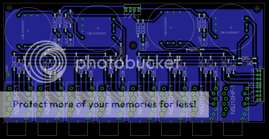
I like 10 mil clearance on pins, which is 0.254mm.  Take the largest tolerance for the pin diameter (it should be 0.64 +- some small number), and add 0.254mm.  This should be the finished hole size (it's the drill diameter plus twice the plating thickness on the holes).

1) Make sure when you submit the Gerbers to the fab house that you are specifying finished hole size and you will be fine.
2) Check every pin diameter against every hole you have in your layout.  Nothing is worse than getting a board back that have holes too small for the components you are using.
3) Make sure you pass a DRC check for rules at least 10% larger than the minimums specified by the board house (e.g. if they specify 10mil minimum trace and 10mil clearance, you should pass on 11mil x 11mil.
4) Make sure the house will step and repeat and depanel for you unless you are real steady with something that saws fiberglass.
5) I would turn on component designations in the silkscreen.
5) Make all the text on your silkscreen at least 10mils or thicker.
 
One tip on my experiences..
Always use bigger or huge pads..small ones are hard to solder...specially on resistors and caps..i do them all over the place now!!
 
I'm wondering if the ground loops surrounding the Neutrik jacks are a problem?  They're small but numerous.  I suppose the answer is "it depends, just try it both ways".  Etch it as is, then see if scraping a break between a 10k resistor per Neutrik jack and the buss makes a difference.
Nobody mentioned the ground loops, which makes me think they don't matter in this instance.  Could someone explain why, or is this just a vague thing you get an eye for?
 
3nity said:
One tip on my experiences..
Always use bigger or huge pads..small ones are hard to solder...specially on resistors and caps..i do them all over the place now!!

+1.

lernith said:
I'm wondering if the ground loops surrounding the Neutrik jacks are a problem?  They're small but numerous.  I suppose the answer is "it depends, just try it both ways".  Etch it as is, then see if scraping a break between a 10k resistor per Neutrik jack and the buss makes a difference.
Nobody mentioned the ground loops, which makes me think they don't matter in this instance.  Could someone explain why, or is this just a vague thing you get an eye for?

It depends on if there's current flowing through there, or if it's just a shield ground. Without seeing a schem, I don't know off the top of my head.
 
Right, so I've increased the hole sizes on the cinemag and neutrik libraries. I'm assuming the standard eagle resistors and capacitors will be fine, or do you recommend increasing their pad/hole sizes as well?

The circuit is just a passive summing network, and that ground will go straight to chassis with no other connections. The top molex header is to go to a make-up stage, whilst the side molex is to go to a bypass switch.

Thanks for all the help
 
It's the resistor/cap pads that look incredibly small to me. I worry about lifting a pad when there's that little amount of copper to absorb the heat while soldering.
 
Back
Top