Critique my PCB layout

GroupDIY Audio Forum

Help Support GroupDIY Audio Forum:

This site may earn a commission from merchant affiliate links, including eBay, Amazon, and others.

jasonallenh

Well-known member
Joined
Dec 6, 2011
Messages
303
Location
All Over Florida
Hi everyone,

I have a surplus of transformers and would find it useful to reuse these 1517s to make the 1520 insert send from the UA8000 desk. I haven't really done a lot of layout work, and vaguely remember some junk about making the input to the amp short and avoiding tangling power with signal. East-West on one side, North-South on the other. That sort of stuff. I'm at a point now where I could just make it go, but I'd appreciate some unkind words just in case I've done some foolish stuff. I have a hunch of what some of that could be, but I'm happy to give you a chance to twist your mustaches. Note that the un-routed traces are part of the ground net and should be gone once I do the ground plane. I left that off for now so my tomfoolery could be more easily exposed. I am thankful for any and all contributions!


1693282306361.png1693282370502.png
 
You need decoupling on the supply rails, something like 0.1uF close to the chip and about 100+uF in parallels.
You may (or not) want to add distribution resistors that would help minimizing the effects og ground loops, if any. Like 10-22 ohms in each supply ingress.
With such a small footprint, "ground" circulation is not a big issue.
 
I'd use thicker traces and / or tear-drop connections to pads for robustness. There's a couple of spots where tracks are very close to pads that I'd space out a bit. Personally, I spend a bit of time making everything look pretty after it's technically correct. Also, don't forget this is a 3D object that exists in the real world, double check that it will fit and is able to be securely mounted in the intended spot.
 
  • Decoupling as already pointed out.
  • Tracks from R18 are thinner than others for no apparent reason.
  • Personally I try to avoid running tracks under components on same side eg R18 here. Although sometimes it's the best way to route.
  • Track from Tx Pin 1 is thinner than others and imo gets too close to transformer pads above it (even if it doesn't violate design rules). Plenty of room there but I would get it out from the transformer footprint area directly and rework the layout to bring it up the side of the tx to R15 / C4
  • Silk Screen - avoid putting text under components as can't read them :) Orientate all text same way. Indicate Tx pin numbers.
 
You need decoupling on the supply rails, something like 0.1uF close to the chip and about 100+uF in parallels.
You may (or not) want to add distribution resistors that would help minimizing the effects og ground loops, if any. Like 10-22 ohms in each supply ingress.
With such a small footprint, "ground" circulation is not a big issue.
I was wondering about the decoupling caps. Are they assumed when the schematic doesn't show the amp's power pins? Only reason I left them off was because I stayed very close to the schematic.
 
You might consider using a double clad board (solid copper on the bottom connected to ground) to provide a ground plane. Then each ground point in the circuit should connect to the bottom with a plated-through hole (PTH) or hand-installed jumper leads if a PTH board breaks the budget.

Order the board with nickel plating on the copper. Specify 2 oz. copper thickness.

Wherever possible keep the traces thick rather than thin (helps with tolerating soldering heat).

The op-amp power pins should include small caps (0.01 to 0.1 uFd) to ground, as close to the amp IC as possible. A 10 Ohm series resistor between each power pin and its source is also a good idea.

This is really a big subject... but hopefully the few ideas I offered are helpful.
 
Last edited:
You might consider using a double clad board (solid copper on the bottom connected to ground) to provide a ground plane. Then each ground point in the circuit should connect to the botton with a plated-through hole (PTH) or hand-installed jumper leads if a PTH board breaks the budget.
There are tracks on both sides so I take it that the board will be copper clad on both sides before etching and the ground planes / fills aren't there yet ?

Order the board with nickel plating on the copper. Specify 2 oz. copper thickness.
What benefit do you think 2 Oz (70um) copper would offer in this application ?

Wherever possible keep the traces thick rather than thin (helps with tolerating soldering heat).

Don't go too far with that though. Thicker tracks can make hand soldering more difficult by acting as heatsink. Depends on soldering control / capability really. Temperature Controlled etc ?
Unless DIY etching, anything down to at least 0.3mm should be fine with any reasonable quality supplier. Not that you need to remove more copper than required.
 
There are tracks on both sides so I take it that the board will be copper clad on both sides before etching and the ground planes / fills aren't there yet ?


What benefit do you think 2 Oz (70um) copper would offer in this application ?


Don't go too far with that though. Thicker tracks can make hand soldering more difficult by acting as heatsink. Depends on soldering control / capability really. Temperature Controlled etc ?
Unless DIY etching, anything down to at least 0.3mm should be fine with any reasonable quality supplier. Not that you need to remove more copper than required.
Oh, I missed the color coding on the traces... So yeah, flood-fill and ground the bottom side where there are no traces.

2 oz copper gives a physically more robust PCB and tolerates soldering heat better with less pad-lifting.

From the physical dimensions (based on the IC footprint) I would think thicker traces would not present a soldering problem. 0.3mm seems unnecessarily thin; it would be appropriate for high pin density SMT ICs like FPGAs. 1 mm (40 mils) would be a decent minimum, especially since there is a transformer present.
 
1) It looks like you could turn the transformer 90 degrees and end up with a lot less wasted space along the top and bottom.

2) Assuming blue = bottom, you have a lot of tracks routed on the bottom that could be on the top. This will clear the way for having a clean ground layout on the bottom, or if you decide to pour ground on the bottom, less breaks/interruptions.

3) Don't be afraid of mixing SMD. The best place to put decoupling is is under the op-amp on the bottom, with the cap connecting across the op amp supply rails with super short traces. You'd just solder the cap right on the bottom underneath the op amp. This works even if you decide to use a DIP socket.

4) (personal preference) I like to rotate all polarized caps so that all of the "+" terminals are pointing towards the same side of the board, to make it easier to stuff the board without having to double check.

5) If you are hand soldering, I would suggest increasing the annular ring width on your PTH's, to aid in solder-ability.

6) Wider pitch input and output connectors are easier to solder (common pitches are 0.2", 3.5mm, and 5mm), or if you decide to use screw terminals, you can use them without changing the layout.
 
Are they assumed when the schematic doesn't show the amp's power pins?

You, you typically would have some capacitors in the schematic connected to the appropriate power rails, with a text note beside the schematic components indicating where they should be placed in the layout. Less important as information transfer when you are drawing schematic and layout, but a nice habit to get into to help other people reading your schematics.
 
You might consider using a double clad board (solid copper on the bottom connected to ground) to provide a ground plane. Then each ground point in the circuit should connect to the bottom with a plated-through hole (PTH) or hand-installed jumper leads if a PTH board breaks the budget.

Order the board with nickel plating on the copper. Specify 2 oz. copper thickness.

Wherever possible keep the traces thick rather than thin (helps with tolerating soldering heat).

The op-amp power pins should include small caps (0.01 to 0.1 uFd) to ground, as close to the amp IC as possible. A 10 Ohm series resistor between each power pin and its source is also a good idea.

This is really a big subject... but hopefully the few ideas I offered are helpful.

Per the original post- I intend to have a ground plane, but I've not put it in yet so that my routing can be seen more clearly. I intended to to do that already.

2oz copper is the default in my EDA.

I think for something like this, 20 mil spaces and traces are what I'm going to end up with, but yes, bigger traces.

Decoupling caps were not on the schematic, but I thought I was going to need them so I actually left some space around the IC/power inlet for those. I was expecting to need them
 
You, you typically would have some capacitors in the schematic connected to the appropriate power rails, with a text note beside the schematic components indicating where they should be placed in the layout. Less important as information transfer when you are drawing schematic and layout, but a nice habit to get into to help other people reading your schematics.

Yep, I found them. Pretty much right on the money with Abbey's recommendation
 
1) It looks like you could turn the transformer 90 degrees and end up with a lot less wasted space along the top and bottom.

2) Assuming blue = bottom, you have a lot of tracks routed on the bottom that could be on the top. This will clear the way for having a clean ground layout on the bottom, or if you decide to pour ground on the bottom, less breaks/interruptions.

3) Don't be afraid of mixing SMD. The best place to put decoupling is is under the op-amp on the bottom, with the cap connecting across the op amp supply rails with super short traces. You'd just solder the cap right on the bottom underneath the op amp. This works even if you decide to use a DIP socket.

4) (personal preference) I like to rotate all polarized caps so that all of the "+" terminals are pointing towards the same side of the board, to make it easier to stuff the board without having to double check.

5) If you are hand soldering, I would suggest increasing the annular ring width on your PTH's, to aid in solder-ability.

6) Wider pitch input and output connectors are easier to solder (common pitches are 0.2", 3.5mm, and 5mm), or if you decide to use screw terminals, you can use them without changing the layout.

1) I was thinking that too. I also got hyper-obsessed with making sure the hot/cold outputs had similar length traces, which I've been told matters? I'm not sure about that. I think I defaulted to the orientation on the schemo, though- I'm not committed to it, and I think turning it like you said will open more space for the components I need to add.

2) I've changed a couple already- definitely going to pursue this.

3) I've actually soldered my little TDK caps to the socket before. They fit, but it's ugly... I have done a very small amount of SMD work but I can probably handle this.

4) I hate the layout symbols I was give, too. I'm definitely going to work this out. I think the first cap at the input is just oriented this way out of an obsession of making the input to the amp as short as possible (another thing I've read that I should be doing)

5) I was definitely planning on this- I've used the default pad sizes and I am able to work with them, but I don't like it!

6) This I'm kind of married to because I have a kit of molex connectors that I want to use up. I like the screw terminals, but I really like the satisfaction of a good crimp 🥴


Hey these are all great comments...no wonder those C12 PCBs are so good!
 
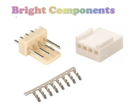
Are you using 0.1" locking connectors like this?

s-l1200.webp

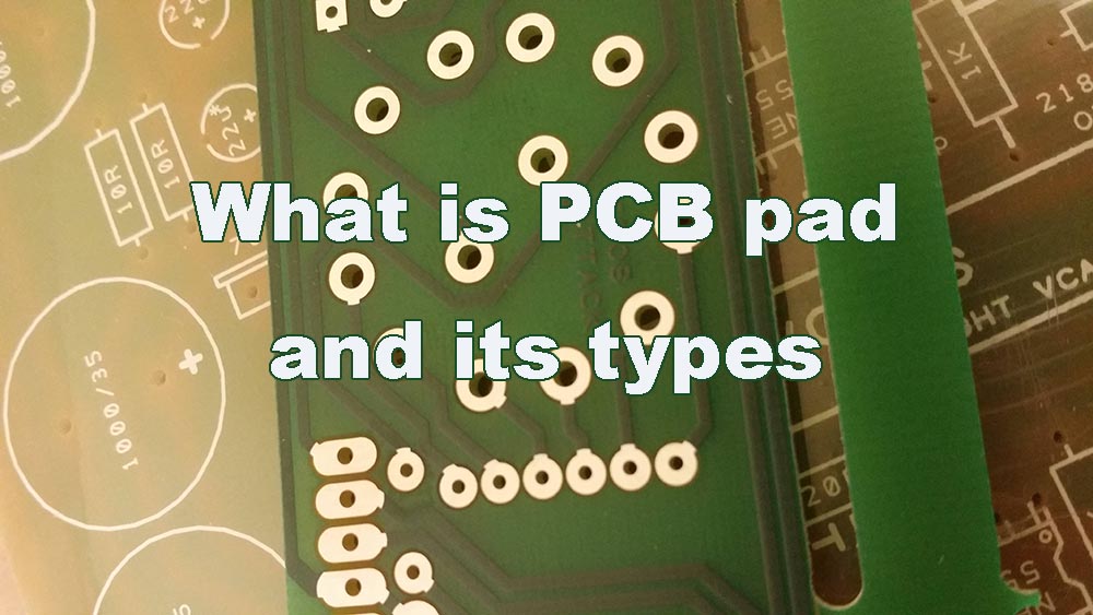
Another trick is to use 'oval' pads (look on bottom left of this layout):

What-is-PCB-pad-and-its-types.jpg


This gives you three connection options:

1) Molex connector: the oblong gives your iron more surface area and makes it easier to solder.
2) Plain wire: you can tin the pad, then lay a wire on it and just solder the wire directly to the pad with no connector. Good for prototyping if you want to remove the wires easily after soldering.
3) Wire in hole: you can stick a wire in the hole, then bend it 90" on the underside, and solder there. Gives both electrical and mechanical strength. Much more difficult to remove.

#2 is my favorite.

Watch for clearances as some board houses have difficult with the thin soldermask between those pads, depending on how wide you set you annular ring.
 
If you chooe #2 from Matador - I would drill a hole next to each of them, that you put the wire through first.
This is a strain relief and prevents broken wires next to where they are soldered in.

Per
 
Oh, I missed the color coding on the traces... So yeah, flood-fill and ground the bottom side where there are no traces.
Easily overlooked on a quick look. And ther are some easy changes to enable a more complete 0V pour on the bottom layer.
Could also pour 0V on the top layer - might not improve anything in practice but it won't hurt and it's better for the environment :)

2 oz copper gives a physically more robust PCB and tolerates soldering heat better with less pad-lifting.

Well I don't envisage this board going into a "harsh environment" and even then I've never seen / judged / experienced a need for it tbh. If you need a more physically robust pcb then imo it's much better to consider a thicker pcb eg 2mm (talking DSPTH rather than multilayer)
If you are getting significant pad lift problems with 35um Cu then I'd say that you have a pcb quality problem and need to find a better pcb supplier. Having the same supplier do 70um Cu is likely just going to get you poor quality 70um Cu pcbs. I'll caveat with that you might look at this if you were envisaging a great deal of desoldering / soldering. But in general with good quality pcbs and decent soldering tools it's not an issue and just a cost without benefit.


From the physical dimensions (based on the IC footprint) I would think thicker traces would not present a soldering problem. 0.3mm seems unnecessarily thin; it would be appropriate for high pin density SMT ICs like FPGAs. 1 mm (40 mils) would be a decent minimum, especially since there is a transformer present.

Maybe I could have been clearer. I'm not saying that the OP should go down to 0.3mm track width here. I was simply pointing out that such track widths are routine so it's not an issue to use thin tracks where it helps routing eg to fit between component legs. Eyeballing it the track width primarily used there looks fine. Maybe increase some of the annular ring sizes a tad.
 
2) Assuming blue = bottom, you have a lot of tracks routed on the bottom that could be on the top. This will clear the way for having a clean ground layout on the bottom, or if you decide to pour ground on the bottom, less breaks/interruptions.
+1

3) Don't be afraid of mixing SMD. The best place to put decoupling is is under the op-amp on the bottom, with the cap connecting across the op amp supply rails with super short traces. You'd just solder the cap right on the bottom underneath the op amp. This works even if you decide to use a DIP socket.
+1

4) (personal preference) I like to rotate all polarized caps so that all of the "+" terminals are pointing towards the same side of the board, to make it easier to stuff the board without having to double check.
+1 although sometimes there's a judgement to be made in terms of layout / signal flow.

5) If you are hand soldering, I would suggest increasing the annular ring width on your PTH's, to aid in solder-ability.
+1

6) Wider pitch input and output connectors are easier to solder (common pitches are 0.2", 3.5mm, and 5mm), or if you decide to use screw terminals, you can use them without changing the layout.
Not really getting this. Considering 2.54mm pitch connectors - you have to deal with similar pitch with thru hole components eg ics all the time so not seeing what the extra problem with connectors would be. imo wider pitch where not required electrically is just taking up pcb estate for no good reason. Maybe not an issue with this pcb but in general. It's personal though - and I do find 2mm 'Hard Metric' oddly tight given that it's only 0.54mm less :)
For my money Molex KK 2.54mm Friction Lock - sorted (as long as you have a good crimp tool and technique or get them done by someone who does).
 
Are you using 0.1" locking connectors like this?

s-l1200.webp

Another trick is to use 'oval' pads (look on bottom left of this layout):


This gives you three connection options:

1) Molex connector: the oblong gives your iron more surface area and makes it easier to solder.
2) Plain wire: you can tin the pad, then lay a wire on it and just solder the wire directly to the pad with no connector. Good for prototyping if you want to remove the wires easily after soldering.
3) Wire in hole: you can stick a wire in the hole, then bend it 90" on the underside, and solder there. Gives both electrical and mechanical strength. Much more difficult to remove.

#2 is my favorite.

Watch for clearances as some board houses have difficult with the thin soldermask between those pads, depending on how wide you set you annular ring.

I laughed at the rainbow text. Yes! "Bright Components!" Those exact ones. Very good point about the oblong pads- #2 will definitely be helpful as I get this thing off the ground.

Not really getting this. Considering 2.54mm pitch connectors - you have to deal with similar pitch with thru hole components eg ics all the time so not seeing what the extra problem with connectors would be. imo wider pitch where not required electrically is just taking up pcb estate for no good reason. Maybe not an issue with this pcb but in general. It's personal though - and I do find 2mm 'Hard Metric' oddly tight given that it's only 0.54mm less :)
For my money Molex KK 2.54mm Friction Lock - sorted (as long as you have a good crimp tool and technique or get them done by someone who does).

I've soldered plenty of DB25 connectors and have no issue soldering in tight space, so I generally don't think much about pad size or spacing, until I start working on one of my boards and realize how annoying it is to be stuck with a tiny pad. The KKs are exactly what I use. Either that or screw terminals, but I currently have an abundance of the former and none of the latter.
 

Latest posts

Back
Top