Moby said:
Here is the preliminary version based on suggestions before. Free for criticism ;D
What Harpo said.
Besides:
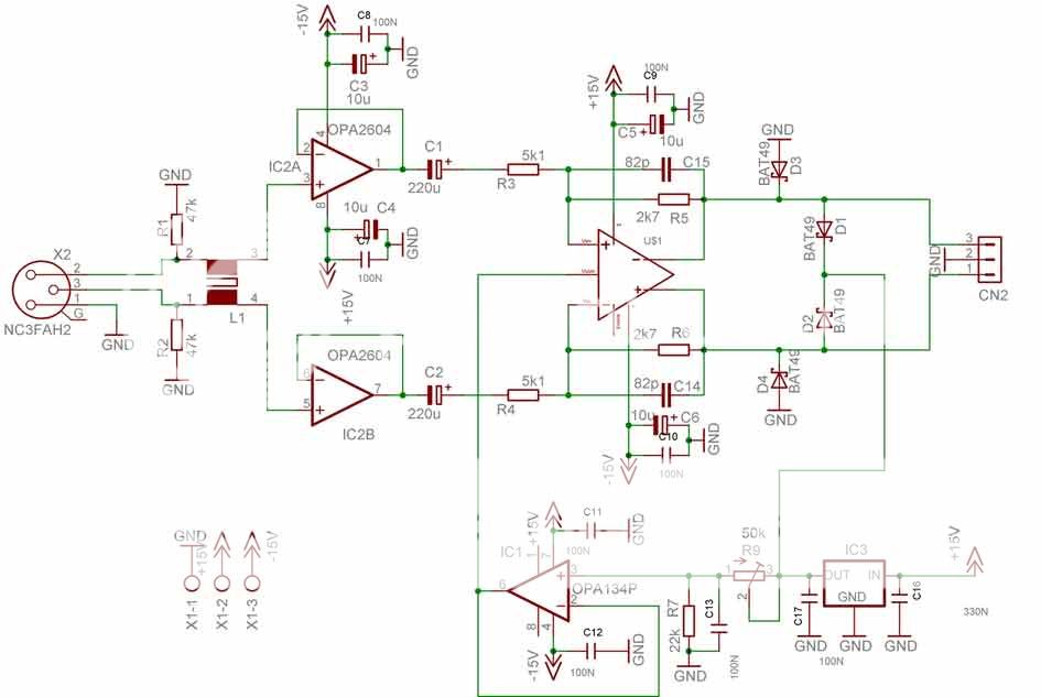
- move the two series resistors (R10A/B on the Beh schematic) to your board, lower them to 68...100Ohm
- remove the shunt resistor (Beh R6); a pad in that location will cost you more in distortion than it gains in noise performance
- if you lower R10A/B, raise Beh C31. Agree with Dan: replace it with a C0G or other high-quality cap
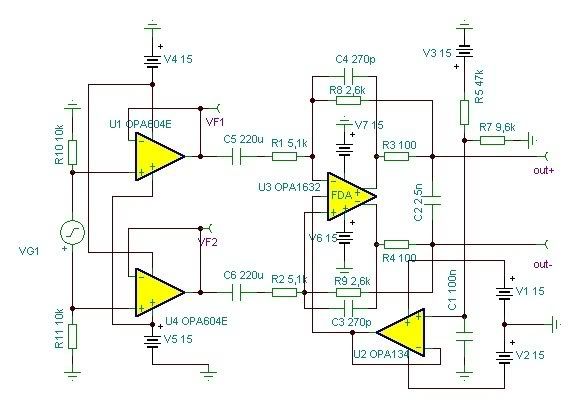
- connect R5/R6 the way you did in your earlier schematic
- most op-amps, including the OPA2604, have much more distortion in non-inverting mode than in inverting mode. Change them to inverting, possibly with a slight loss (~6dB) to allow for larger input swings
- move C1/C2 before the OPA2604s. The small DC offset of the 2604s will most likely not matter much. Better yet, replace the OPA2604 with a proper line receiver like
the THAT12xx series.
- the protection diodes D1-D4
must be on the same board as the converter, with minimal trace length to the converter's power and ground lines. Your IC3 is likely a standard linear regulator; these can't sink current, so there's nothing stopping the OPA1632 from pulling IC3's output up through the protection diodes.
- set your total system gain (or more likely loss) to adapt expected line levels to your converter's input. With the values you have it looks like the converter clips when the input is ~20dBu, does that offer you enough headroom?
- the OPA1632 runs pretty hot at +/-15V; consider running it at a lower voltage.
About your PCB:
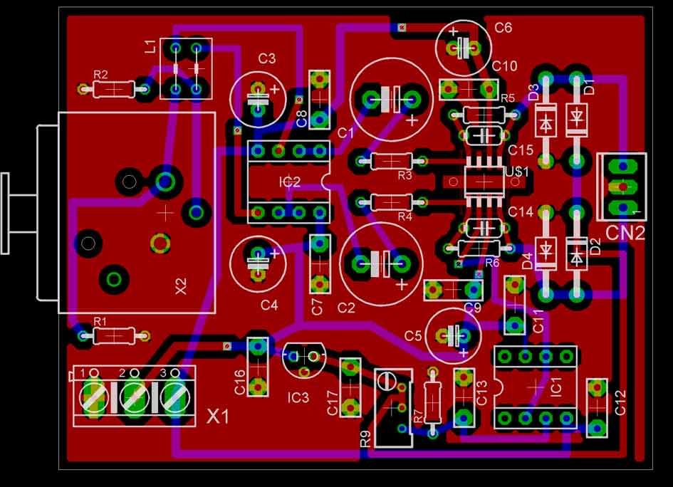
- the decoupling capacitors are
much too far from the OPA1632. Use SMD ceramics; try to place them as close to the chip as possible.
- have a contiguous ground plane on one side of the board
- I would suggest also using a good (=C0G) SMD cap for C14/C15
JDB.


")