GDIY boost converter for HT B+

GroupDIY Audio Forum

Help Support GroupDIY Audio Forum:

This site may earn a commission from merchant affiliate links, including eBay, Amazon, and others.
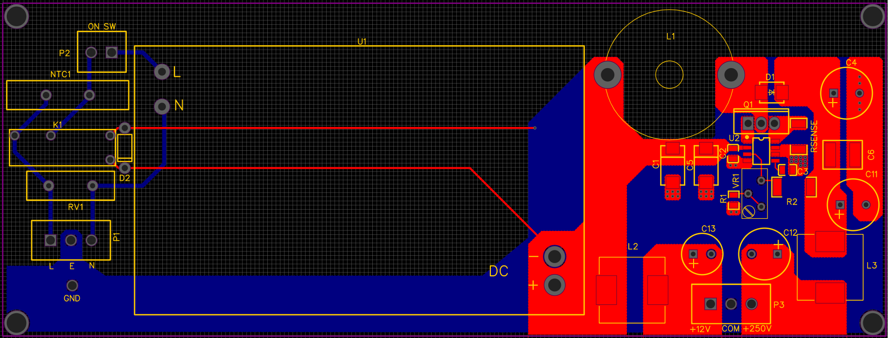
Ok, so I've been reading through the datasheet a bit, here's rev 2.

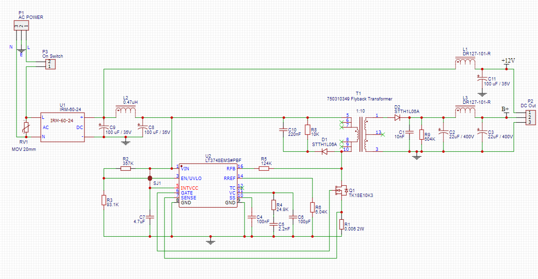
Had to go up on the transformer size from the datasheet, but the Wurth transformer (PN 750310349) seems perfect for the job (near as I can tell). Not sure if this method of using inductors to isolate the "clean" 12V for heaters from the "dirty" 12V for the flyback transformer will work - open to feedback there.

Other values like RFB, Rsense, etc. have been selected to produce 250VDC out, and this should accommodate roughly 230 mA on the HT - which seems like more than plenty.

Maximum current should be 16A in the MOSFET / primary. The primary inductance of the transformer is 5 uH, while this requires a minimum of 4 uH - so "seems" ok.

Minimum load in the datasheet is ~2%, which in this case would be ~5 mA. You could add a zener to establish that load.

One thing I'm not sure about is the jumper between pins 1 and 5 on the LT3748. This is the INTVcc pin, and the datasheet says it "may" be connected if no third winding is used and Vin < 20V. I don't know whether "may" means "should"?

MTzkw2y.png


Thoughts? Comments? Complaints?  ;D
 
I did a layout. Open for feedback.

https://www.dropbox.com/sh/mofsrn4h8pl1gwr/AABZIZKS4Qt4zIiEb_JhlT8-a?dl=0
 
Matador said:
I posted a design several years ago that I made a pcb for and confirmed the design.  Was meant for 12VDC up to 250V at about 10mA (but can go to 50mA with better parts).  Based on MAX1771 and based on requirements from here:

https://desmith.net/NMdS/Electronics/NixiePSU.html

I notice this design achieves an output ripple of about 1% which is fine for Nixie tubes. Since nearly all tube preamps have a very poor PSRR this amount of ripple is much to high. It needs to be at least 60dB lower for a mic pre for example. Did you apply any further filtering and what level of ripple did you achieve?

Cheers

Ian
 
ruffrecords said:
I notice this design achieves an output ripple of about 1% which is fine for Nixie tubes. Since nearly all tube preamps have a very poor PSRR this amount of ripple is much to high. It needs to be at least 60dB lower for a mic pre for example. Did you apply any further filtering and what level of ripple did you achieve?
A few things:  first, the ripple frequency is way up over the audio band, somewhere between 60kHz and 85kHz, depending on load.  So even small RC filtering is very effective at reducing it (for example, even at the lowest switching frequency, 100 Ohms into 47uF is 65 dB down).  Second, in my design, I added a CLC filter to the output, and measured somewhere around 2mV under load (10mA), when set to 200V output.  My design used the shielded inductor and thus efficiency was around 80%.  It was powered from a very common 19.5V, 3A wall wart which are very inexpensive and plentiful.

I think I still have scope pictures somewhere, if interested.
 
That design seems to be limited by the transformer, which only has a secondary current rating of 2mA, 200V. The high value of the current sense resistor limits the peak current.

There's a relationship between primary inductance, saturation current, ratio, the size of the current sense resistor, and the duty cycle. I only found one transformer that seems to suit, but it has low primary inductance (only 5 uH) which means the sense resistor has to be small (6 mohm) and, which makes the current limit high (16.7 A).

I don't have much intuition if this is adding up, but I'm skeptical. The maximum current seems very high. The maximum output current set by Rsense, the transformer ratio, and duty cycle would be .230 mA or so, but that requires 13 amps rms which seems silly.

Without any real world experience though I think I'm at about the limit of my ability.
 
Matador said:
I posted a design several years ago that I made a pcb for and confirmed the design.  Was meant for 12VDC up to 250V at about 10mA (but can go to 50mA with better parts).  Based on MAX1771 and based on requirements from here:

https://desmith.net/NMdS/Electronics/NixiePSU.html

Thanks for sharing this, seems like a more reasonable solution than the isolated version.
 
dogears said:
Thanks for sharing this, seems like a more reasonable solution than the isolated version.
Unsure how "reasonable" it is  ;D, because fully isolated has some distinct advantages.  However flyback topologies can be quite finicky and require a lot of experience to tune properly:  at a previous job I was surrounded by a team of PhD's who dedicated their careers to understanding them and I'm light years away from that.

However the MAX1771 design is quite simple, with an (typically) inexpensive BOM, however it took three iterations of PCB's to get it right, because the layout is very demanding.  The article I linked goes into a lot of detail, but everything matters, and the feedback pin is extremely sensitive to stray EMI, and it oscillates very easy, and you can't just LPF the feedback path because then it won't reliably start up.

If anyone is interested I can share what I came up with.  Nick posted everything you need in that link and you can copy it directly to test it out.  My layout ended up being 1.5" square, which is cool because it's small enough you can even stuff it inside of a guitar pedal.
 

Attachments

  • PXL_20201020_201612851.jpg
    PXL_20201020_201612851.jpg
    262.8 KB · Views: 10
Matador said:
A few things:  first, the ripple frequency is way up over the audio band, somewhere between 60kHz and 85kHz, depending on load.  So even small RC filtering is very effective at reducing it (for example, even at the lowest switching frequency, 100 Ohms into 47uF is 65 dB down).  Second, in my design, I added a CLC filter to the output, and measured somewhere around 2mV under load (10mA), when set to 200V output.  My design used the shielded inductor and thus efficiency was around 80%.  It was powered from a very common 19.5V, 3A wall wart which are very inexpensive and plentiful.
Excellent points
I think I still have scope pictures somewhere, if interested.
Yes please

Cheers

Ian
 
Well ok then, hows this look? Schematic attached, and the layout was as close as I could get to his.

xdxqHYL.png


Attachments

  • Schematic_IA-HT SMPS_2020-10-20_16-10-56.pdf
    50.5 KB · Views: 6
How does the mosfet switching on the output of another (isolated) smps work or interact?

Would the output impedance of the supply switcher limit the max current available to the downstream device? Taking on multiple amps of current through the downstream mosfet seems like it might pose a challenge. 
 
Abbey, I had to calculate the C / Q / I / t to prove it to myself but of course you're right. 100 uF decoupling is plenty.

Still checking my work and I'm not sure I buy this yet.

The MAX1771 datasheet gives a t ON max of 16 uS and t OFF min 2.3 uS, which is a maximum duty cycle of 87% if I'm not mistaken. The guy who's built the thing has done 15V to 187V which indicates a perfectly efficient duty cycle of 92%, so I may be doing something wrong. However, other than that the numbers work out - he used 4A Imax (Rsense = 25 mOhm and the chip's fixed 100 mV current limit) using a 47 uH inductor, to get an output of around 110 mA. This works out to a fosc of around 60kHz.

If we assume everything works the same at the higher voltage we'd expect something around 85 mA max at 250V. But is that possible? 12-250V is a duty cycle of over 95%.

Also, checking the feedback voltage divider as drawn his Vout can only get up to 180V or so.

Matador, you mentioned you can't help the instability on the feedback pin - the datasheet says "In adjustable output voltage and non-bootstrapped modes, parallel a 47pF to 220pF capacitor across R2 (feedback resistor), as shown in Figures 2 and 3. Choose the lowest capacitor value that insures stability; high capacitance values may degrade line regulation."
 
dogears said:
Matador, you mentioned you can't help the instability on the feedback pin - the datasheet says "In adjustable output voltage and non-bootstrapped modes, parallel a 47pF to 220pF capacitor across R2 (feedback resistor), as shown in Figures 2 and 3. Choose the lowest capacitor value that insures stability; high capacitance values may degrade line regulation."
It's because of the large step-up:  in order to get the output voltage close to the reference voltage, you need a very large value (somewhere around 1.5M to 2M) for R2.  With the recommended 47pF, this forms a LPF of 2kHz which is way below the recommended 12kHz (100pF on 140kOhm).  In order to get the same 12kHz LPF in the feedback network, you need something like 4.7pF which is already in the realm of the stray capacitances of the layout itself.

If you find you need it (I never found it necessary once the layout was right), you can also solder a small MLCC 0805 cap directly on top of R2.

Regarding output current, the FET and inductor are the main limiting values.  I think I pulled between 25 and 30mA from mine without issue, however the RDS(on) of the FET limits the output current before the inductor in most cases.  FET prices go up with the cube of smaller RDS(on), so make sure you need that kind of output current before you upgrade.  ;D Mouser has a lot of 25mOhm, 500V MOSFET's you can try, all in the $25 a piece range.
 
Duh, of course that makes sense. I missed the 12kHz recommendation. Thanks.

I'm not worried about output current as much as voltage. There is a limit to the voltage you can develop based on the maximum duty cycle of the controller right?

Good point about VDS max, I picked the current MOSFET based on his (lower voltage) circuit and VDS max was 250V. Womp womp.

IXFP26N30X3 (300 VDss) looks like a good choice for $3.
RDS(on) 53 mOhm
Coss 225 pF
Crss 1 pF
Qg 22 nC
 
dogears said:
I'm not worried about output current as much as voltage. There is a limit to the voltage you can develop based on the maximum duty cycle of the controller right?
The answer is complicated, but most duty cycle equations assume underneath that the steady state load current is enough to maintain the FET in continuous mode (e.g., the inductor current never drops to zero).  Thus the output voltage is strictly set by the duty cycle.  In discontinuous conduction mode (DCM), output voltage becomes a function of load current, the inductor value, and the switching frequency. 

To make a long story short, at light loads, output voltage can be much higher at a lower switching frequency, and becomes limited by component rating, etc.  This is especially apparently for high voltage supplies for capsule polarization supplies, which are essentially capacitive loads with no DC current requirement.

EDIT: this link explains it better than I can.

https://www.ti.com.cn/cn/lit/pdf/slva061
 
Matador said:
The answer is complicated, but most duty cycle equations assume underneath that the steady state load current is enough to maintain the FET in continuous mode (e.g., the FET current never drops to zero).  Thus the output voltage is strictly set by the duty cycle.  In discontinuous conduction mode (DCM), output voltage becomes a function of load current, the inductor value, and the switching frequency. 

I am puzzled. I do  not understand how the FET current can never drop to zero. Surely it has to for the inductor back emf to create the output voltage. Did you mean the Inductor current never falls to  zero?

Cheers

Ian
 

Latest posts

Back
Top