Here is some data I took on a few FET's. The plan is that I'll mock up the front end of this circuit so we can see how these parameters play into the operation of the circuit.
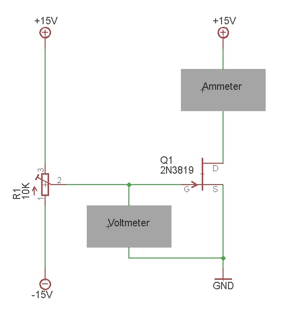
I started by breadboarding up a simple test rig:
You first dial in the pot (a multi-turn precision type works best for this so you can dial in voltages accurately) to show 0V on the voltmeter. This should happen roughly half way through the range of travel. You can then connect the JFET and read the IDSS on the ammeter directly. Note this value down.
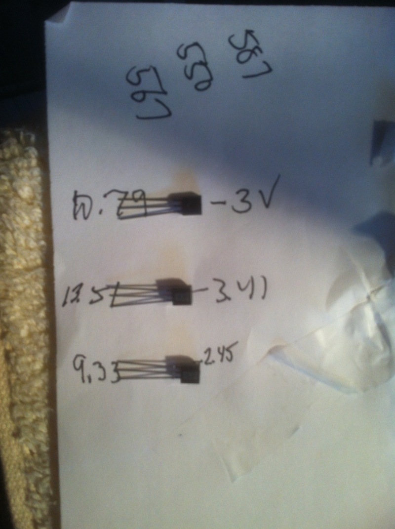
Now we want to figure out VP: dial the pot so that the voltage becomes negative. As you make the voltage more and more negative, you'll see the current drop as the device becomes more and more pinched off. What you want to do is lower the voltage until the current drops to 10% of it's IDSS value. Note this negative VGS value down as well. Repeat these two measurements for all the devices you want to measure. Here are results for the first three JFET's I had in my stash:
Now VP is difficult to measure exactly, as it's defined as the gate-source bias that results in zero drain-source current. It's difficult to measure no current, but we can use the characteristic equation of the JFET to get very close:
ID = IDSS * [1 - VGS/VP]2
If you solve for VP, you get:
VP = VGS/(1 - SQRT(ID/IDSS))
So you have all the above information from your measurements, which results in the following data for these three devices:
Code:
IDSS	ID	VGS	VP
-----------------------------------------------------
10.79	1.079	-3	-4.387425887
13.51	1.351	-3.41	-4.987040758
9.33	0.933	-2.45	-3.583064474
This way of calculating VP is not perfect but I've found it gets pretty close. In general, IDSS and VP track together very well, meaning that the higher the current, the more negative the pinch-off voltage.
So I'm going to pick through 20 or so 2N3819's and 20 or so 2SK170BL's, and find one of each at the high and low ranges of these parameters, then I'll construct the front end of the circuit so we can see what the gain and input ranges look like.
As a primer: gm (or transconductance) is defined as the delta change in ID with a delta change in VGS. Mathematically, this is just the derivative of the ID equation above with respect to VGS. The result is this equation for gm:
gm = | 2 * IDSS/VP * [1 - VGS/VP]
The first interesting result is that gm is a linear function of VGS (and the other parameters as well, which are generally constants). People tend to think of transconductance as a constant but it isn't in this case! It also means that the transconductance is maximum the closer VGS is to zero. These equations can be found in any standard text on amplifier circuits BTW.
For the U87, the basic gain equation for the front end (assuming bypassed source resistor) is:
AV = - gm * RD
So gain is maximized when gm is maximized, which means we should keep VGS as high as possible and operate the JFET as close to IDSS as possible.


") ,
,