Ok here are some more notes about this circuit that I've formulated over the last few days. The equations that govern JFET behavior (and this circuit as an extension), are non-linear and difficult to summarize succinctly. However there are a few broad generalizations that can be made.
First off, we can reason a bit about operating points based on the original Neumann design. First off, it stands to reason that the target was that the drain voltage would sit at roughly half the supply voltage (in this case, this is the voltage coming out of R14, and shown to be 21V). If this is true, then half of this is 10.5V. With a 47K drain resistor, this gives a quiescent bias current of 223uA. I'm guessing Neumann selected 225uA which is really close.
With the drain bias and drain resistor selected, we need to figure out the idling point next. I'll spare the detailed math, but you essentially look at the VGS / IDS transfer curve, and find a point roughly around the point that intersects 225uA. I've found for the nominal 2N3819, this voltage is roughly -3.4V (but given JFET parameter swing, can be anyplace from -0.2V up to damn near -7V!). If you measure the IDSS and IDS points you can calculate VP, then use the equations I provided earlier to find the VGS that intersects with the 225uA point with a spreadsheet.
So if the nominal 2N3819 has a VGS at -3.4V at a quiescent current of 225uA, then the source resistor needs to be 15.2K. This will place the source voltage at 3.4V. With a 47K drain resistor, the drain will idle at 10.5V given these nominal JFET conditions, which I have confirmed with a SPICE simulation.
Herein lies the first problem with this circuit: in order to be in the saturation region, the VDS voltage must be held above VP, otherwise the JFET is operating in it's ohmic (or triode) region. In this region, the drain->source current starts to depend on VDS (and not just on VGS). As the VDS falls, the transistor impedance rises, which can be thought of as a "softening" of the pulling ability of the JFET down towards it's source terminal (it essentially becomes a VCR, or "voltage controlled resistor").
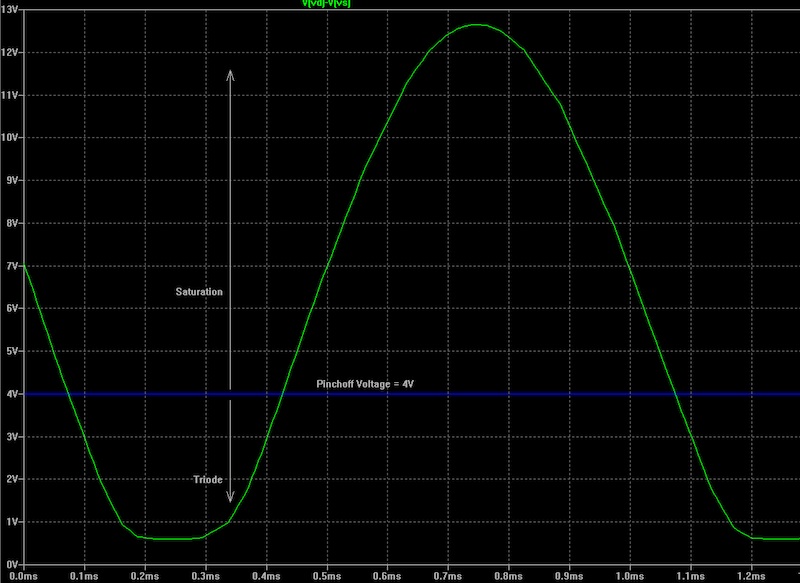
In any case, we must maintain VDS at greater than VP (which in this case is 4V for the nominal 2N3819). Now while the trouble is on the downward slope for output (meaning on the upward slope on the input, given this is an inverting stage), due to the action of gm against RD, the drain voltage will fall "faster" than the source voltage. If this difference falls below VP, the waveform will start suffering a lot of THD.
You can see this for the nominal U87 circuit with a nominal JFET in the SPICE plot below:
which is a plot of VDS with an input signal of 1kHz, 200mV peak to peak. You can see that as the output signal falls below the 4V threshold, the signal flattens out.
This means that the VP level greatly reduces the amount of gain we can realize while still maintaining low distortion. Although the gain calculates at roughly 35, we can really only make use of the first 88mV of input signal before the stage begins to run out of signal swing headroom.
There are two ways this can be mitigated: the first is to run higher quiescent current. This has the effect of reducing the VGS bias, which means that the source resistor can be smaller. With less VGS bias, we can swing more signal. This has the secondary effect of reducing gain however, but we do get more input headroom.
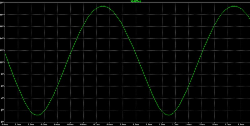
The other way is to jack up the VDD voltage from 21V. For example, if we raise this up to 30V, and idle at 15V, then we can raise up the drain resistor to 67K and have a few more volts of headroom before we start to run into trouble. We have to be careful however, as if we exceed the maximum drain to gate voltage (25V for the 2N3819) we get into more trouble. 30V is about as high as one can go.
Here is the same plot with 30V VDD, 15V idle:
Looks much cleaner, gain is slightly higher as well (50 versus 35, with a larger input swing too). Output impedance is higher however, which means we have to think about dampening into the output transformer too!
The fundamental problem here is that with a nominal JFET, we are operating too far away from IDSS. With IDSS also comes lower VP, which means less headroom.
Here is the same idea with a minimal JFET (2mA IDSS, VP of -0.22V). Gain is up another full order of magnitude (around 100), and we have tons more output swing to use up because VGS is so low (about -0.15V). Gain is up because we are so much closer to IDSS in the quiescent state. The simulation shows that 30mV at the input swings nearly 7V at the output.
However input headroom is tiny: roughly 50mV will take the output to the rail. This may be ok if you are only room miking at a distance, but this would distort heavily on loud sources I am guessing.
What I'll do next is post a chart of IDSS and VP, and what the gain and headroom look like. That way, you can hand select a JFET to go with whatever operation you like. I'll also post the source resistor values so that those without a scope can get very close to the ideal value.




![Soldering Iron Kit, 120W LED Digital Advanced Solder Iron Soldering Gun kit, 110V Welding Tools, Smart Temperature Control [356℉-932℉], Extra 5pcs Tips, Auto Sleep, Temp Calibration, Orange](https://m.media-amazon.com/images/I/51sFKu9SdeL._SL500_.jpg)


