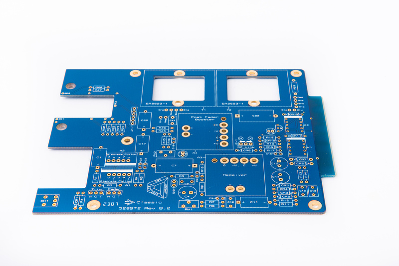
[BUILD] CAPI VC528 ML2~500 Series~Missing Link 2~Official Support Thread

GroupDIY Audio Forum

Help Support GroupDIY Audio Forum:

This site may earn a commission from merchant affiliate links, including eBay, Amazon, and others.

jsteiger

Well-known member
White Market Member
Joined
Apr 11, 2008
Messages
3,586
Location
Nashville TN
Since the kits have started shipping, it's time for the support thread!  :)

**This is a somewhat complicated build. A touch harder than a VP28 but easier than a Love Child. I recommend reading completely thru the Assembly Aid before starting on anything. There are some points made in the doc that can save you much time and prevent crucial errors during the build.

**Resident build/pic/blogging expert 'Chunger will be working his magic on a build sometime soon. His wonderful photo pics will be in the posts immediately following this one. In the meantime, please use my pdf Assembly Aid for your builds.

--------------------------------------------------------------------------------------------------------
September 21st, 2015 Update:
All support docs for this project can be found on the recently added
Support Docs page at www.capi-gear.com
--------------------------------------------------------------------------------------------------------


Some details can be found here http://capi-gear.com/catalog/product_info.php?cPath=22_117_120&products_id=222

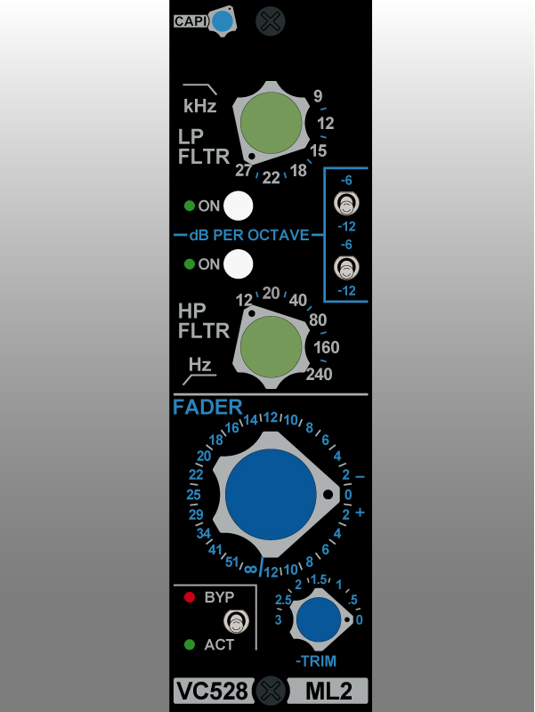
temp-ML2.jpg


Cheers, Jeff
 
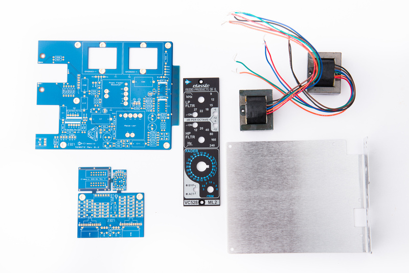
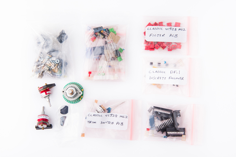
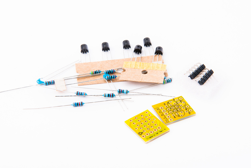
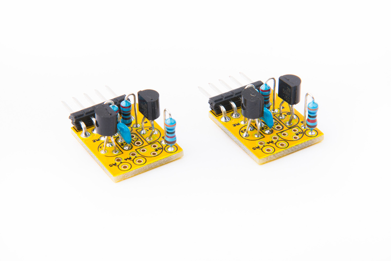
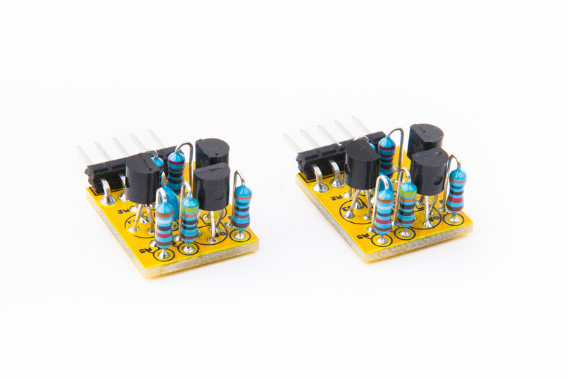
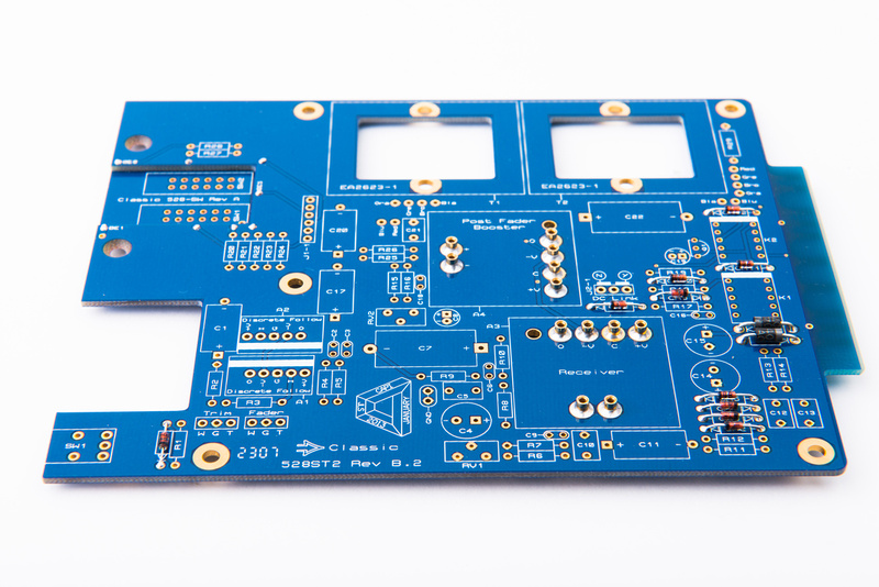
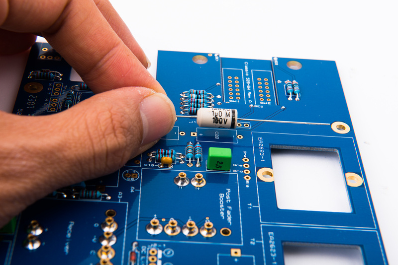
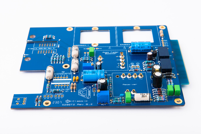
OK. . . a bit late to the party, but here is a walk-through of the ML2 build top to bottom.  First, let's have a look at the kit components as they come out of the box.  This revision really simplifies the assembly of the Missing Link units and moves this kit from one of the more difficult and involved CAPI builds to an exponentially easier project.

p638770515-4.jpg


p753984720-4.jpg


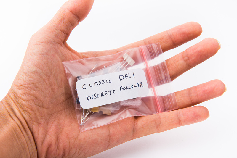
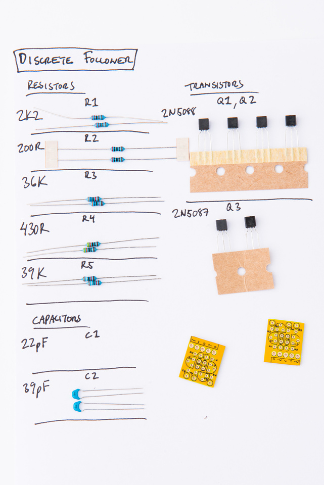
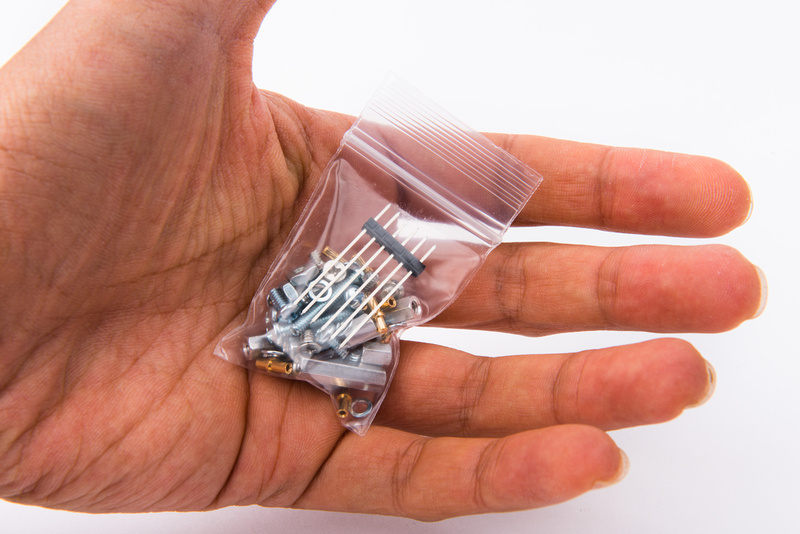
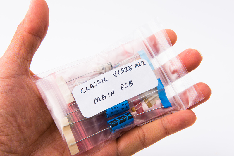
First, assemble the 2 discrete follower boards.  The parts are contained in this bag.

p583922540-4.jpg


p959539848-4.jpg


It is helpful to organize and sort the parts before assembly.

p753871626-6.jpg


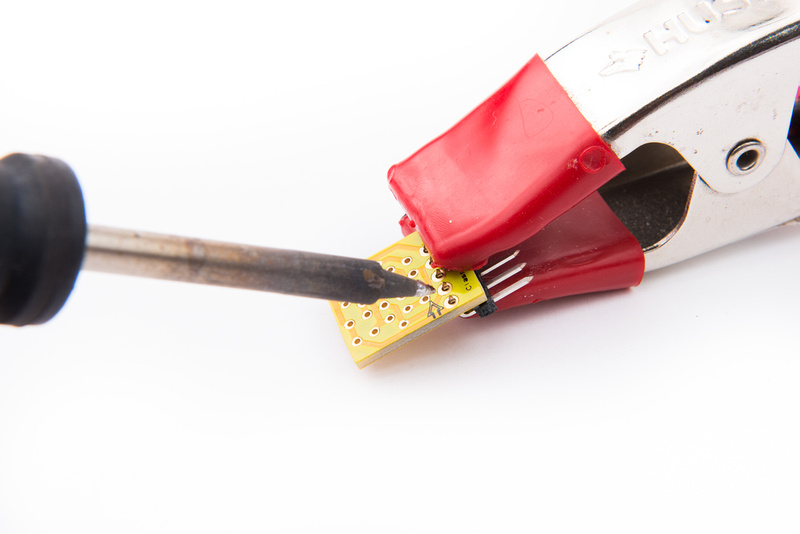
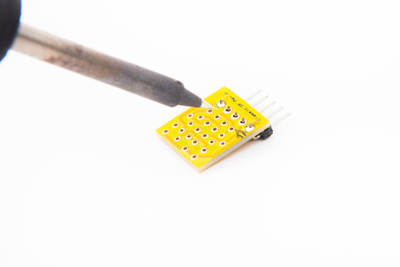
Once all of the components are identified, begin by installing the header.  I clamp the header tight to the PCB and leave 2 pins exposed on one side and solder those first.

p1006343920-4.jpg


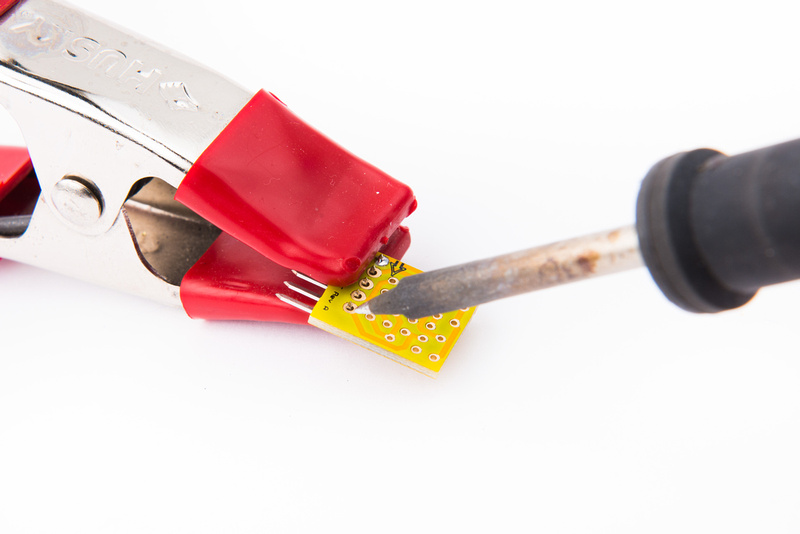
Then, re-position the clamp to expose 2 pins on the opposite side and solder.

p820266412-4.jpg


And solder the pins  in the middle with the clamp removed after the outer 4 pins are secured.

p1011262126-4.jpg


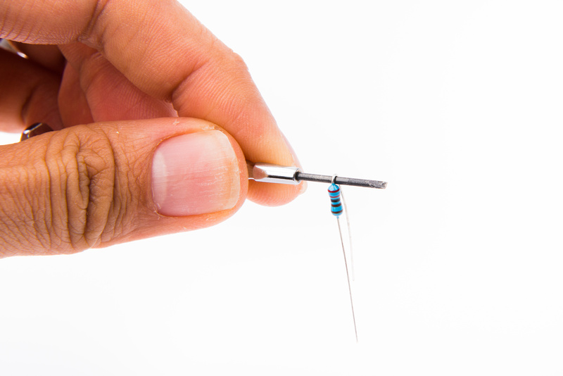
A convenient way to bend the resistors for vertical mounting is to use a small screwdriver .

p700033559-4.jpg


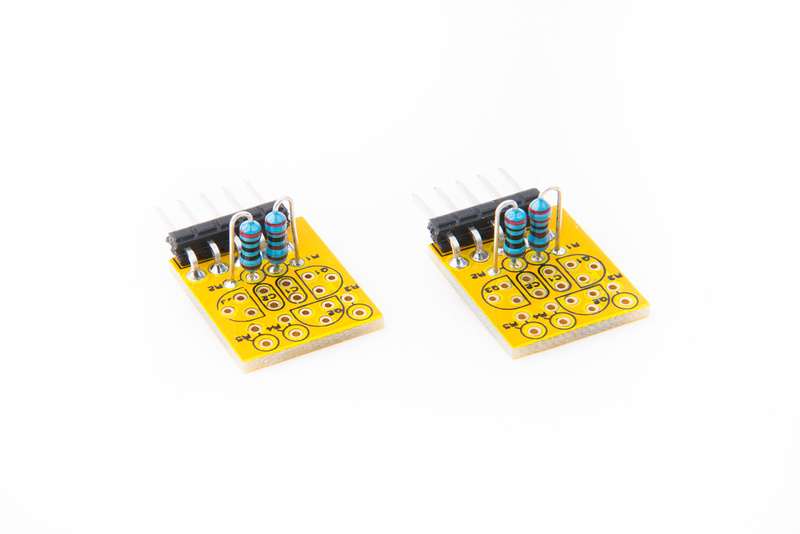
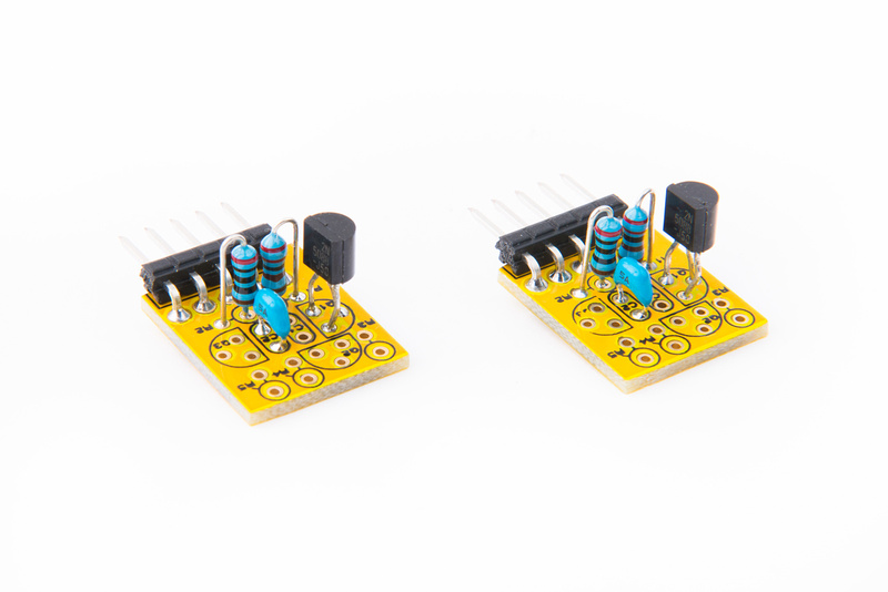
And, we populate the discrete follower PCB's according to the BOM and silk screen markings.

p791309424-4.jpg


p285757606-4.jpg


p119452973-4.jpg


p203464503-4.jpg


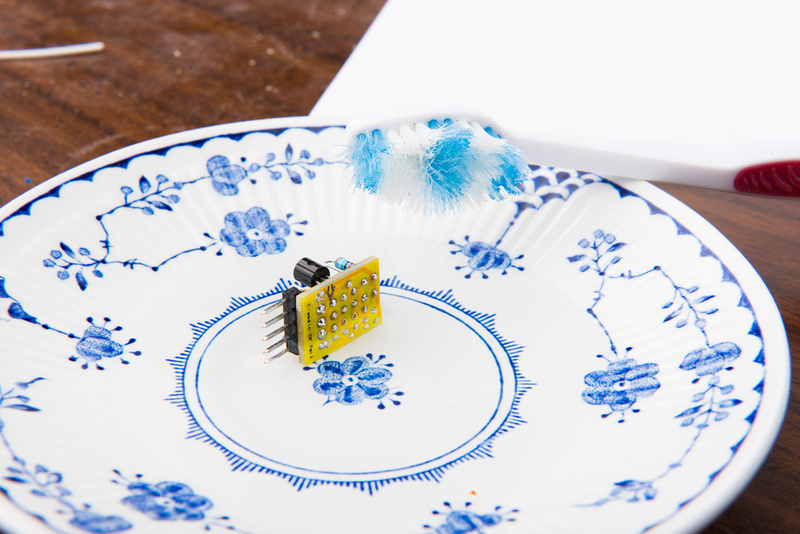
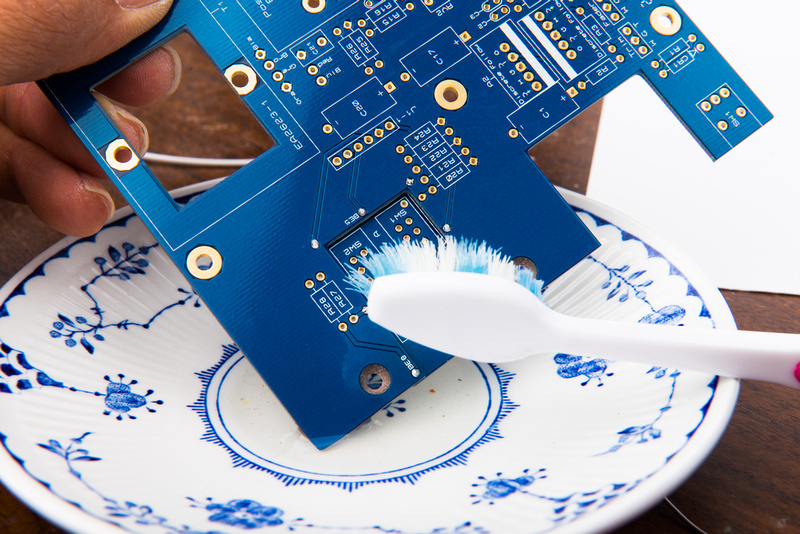
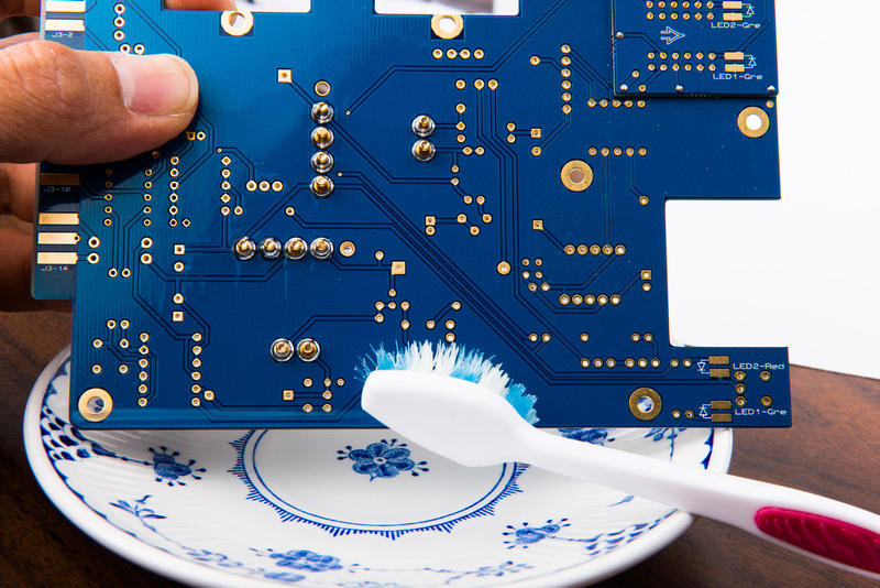
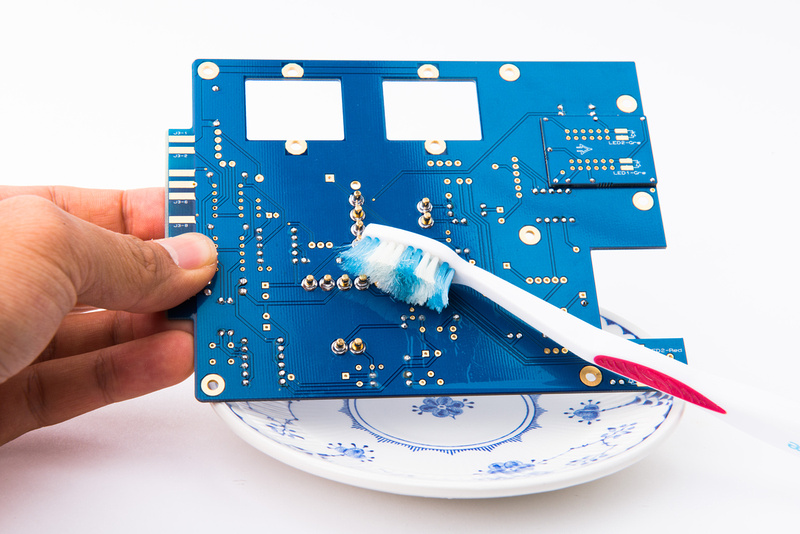
It is probably optional in this particular build, but I use some 90% isopropyl alcohol and a toothbrush to dunk and scrub the PCB's to remove all of the solder flux.  None of the components on the discrete follower PCB are susceptible to damage from the IPA solution.  If you do decide to clean the board, do not go half way and just dab a few drops of alcohol on the board.  It will just smudge the flux everywhere and make a sticky mess.  Commit and scrub the back side down thoroughly with a toothbrush until all of the flux is dissolved and removed.

p44160965-6.jpg


p405191274-4.jpg


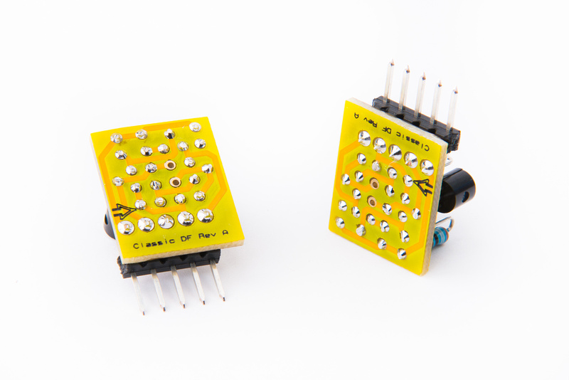
Discrete follower boards assembled and all cleaned up.

p147662668-4.jpg


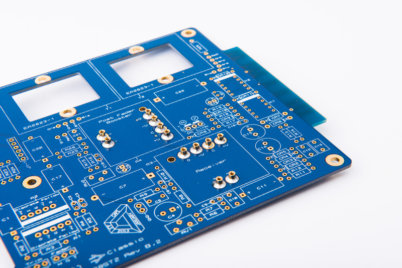
Next, we procede to the main PCB.

p271683667-4.jpg


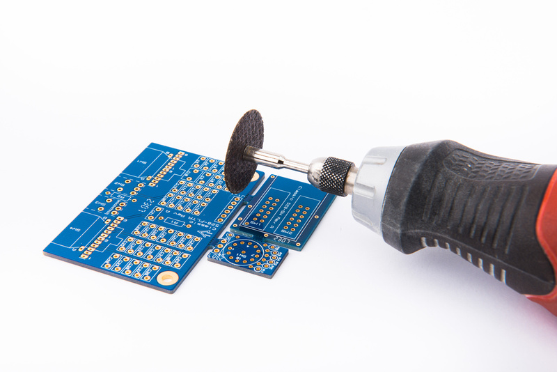
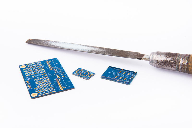
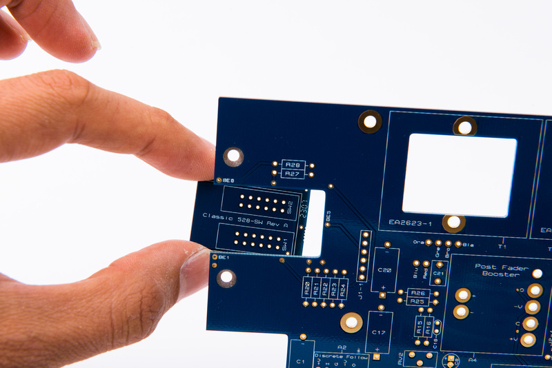
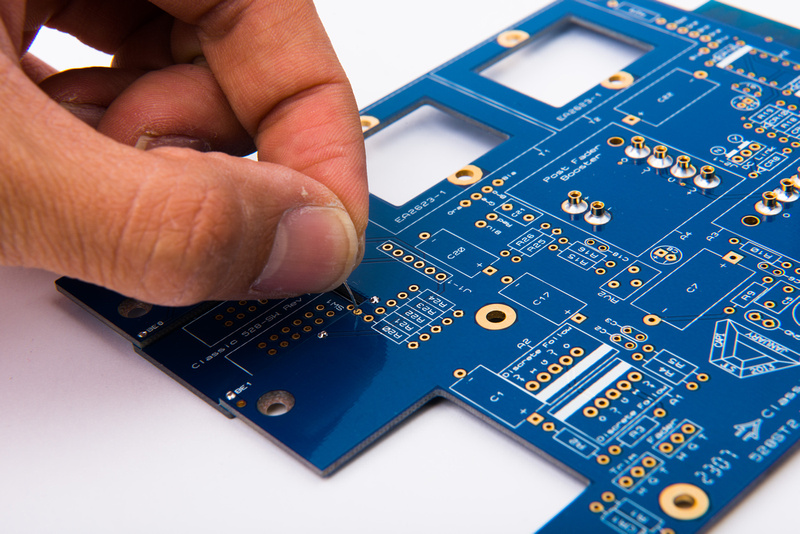
The first step in assembling the main PCB is to attache a small sub-PCB for switches.  So, start by cutting apart the sub-PCB's and cleaning up the edges with a file.

p411900231-4.jpg


p173112781-4.jpg


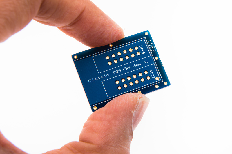
This is the board we are after.

p19107180-4.jpg


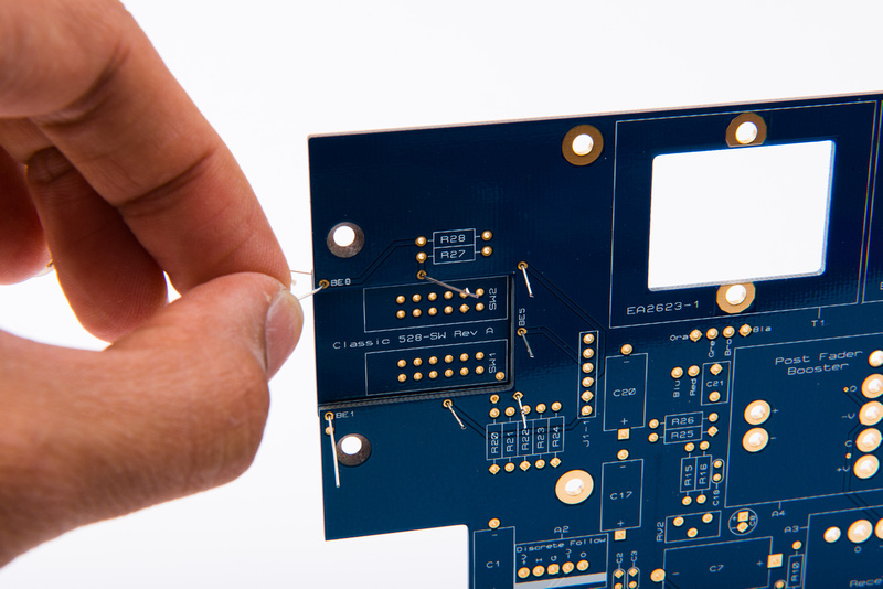
And it fits onto the main PCB like this:

p442032326-4.jpg


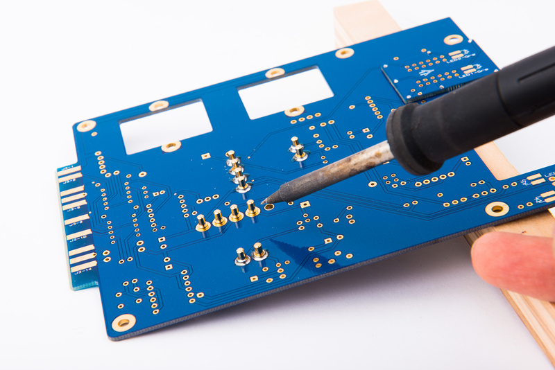
The board is mounted via plated through holes with component cut-off leads.

p222297025-4.jpg


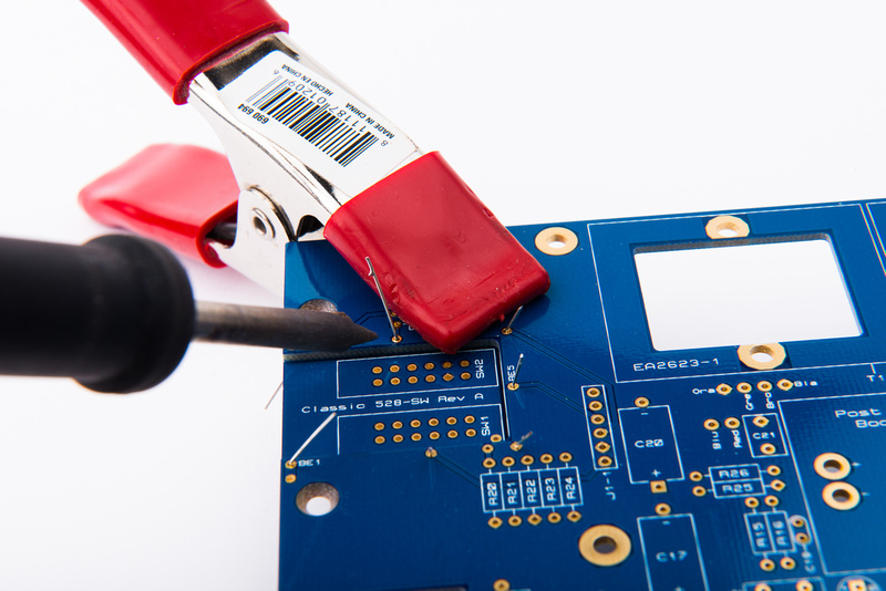
Once the leads are set in place, the board can be clamped and soldered.

p31915777-4.jpg


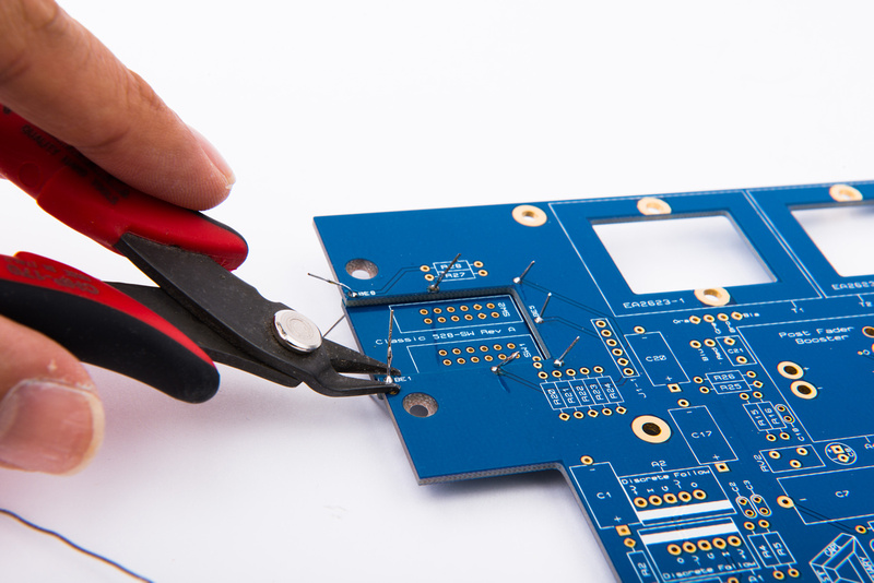
And the excess trimmed off.

p460157396-4.jpg


If you have decided to clean off the solder flux from the boards, now is as good a time as any to scrub off the flux with 90% IPA solution.

p521915478-4.jpg


Next, locate the small bag containing the hardware.

p269433378-4.jpg


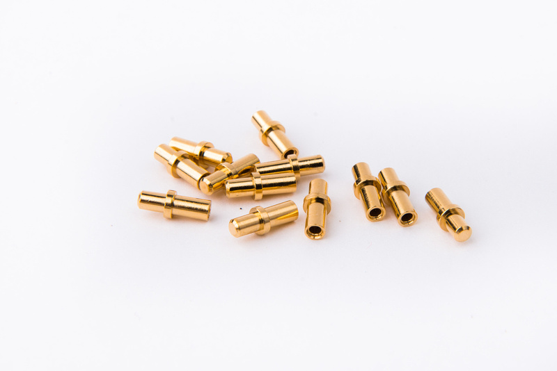
And locate the discrete op-amp sockets.

p50916462-4.jpg


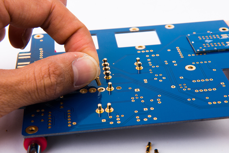
Insert into the main PCB from the back side and solder in place.  Note: significant heat may be needed to get these pins started.  Aim to flow enough solder into the sockets to bleed onto the back side, but not so much that it goes all the way down and intrudes into the actual pin interface area.

p332249735-4.jpg


p209863080-4.jpg


p331048704-4.jpg


And, while there are few components on the main PCB, it is easy to scrub flux off of the board at this stage.

p459808413-4.jpg


I also noticed that I missed one junction point for the sub-PCB that mounts the push switches, so I insert that now.

p336444005-4.jpg


Next, locate the bag with the electronic components to populate the main PCB.

p323532555-4.jpg


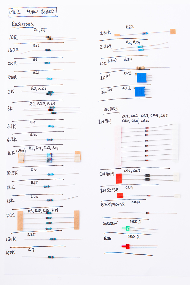
And, we identify the components and organize them for easy access to avoid mistakes.

p1035137463-6.jpg


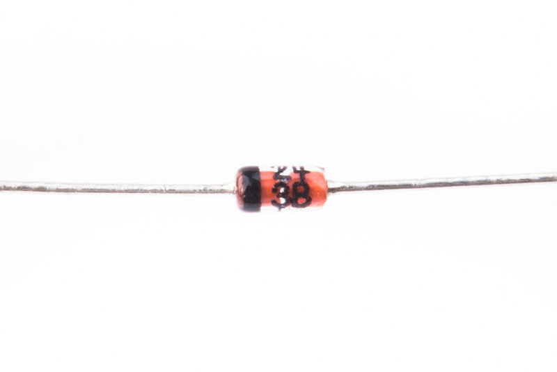
Pay particular attention to the small diodes because the markings are very hard to read.  CR9 looks like this:

p958837975-4.jpg


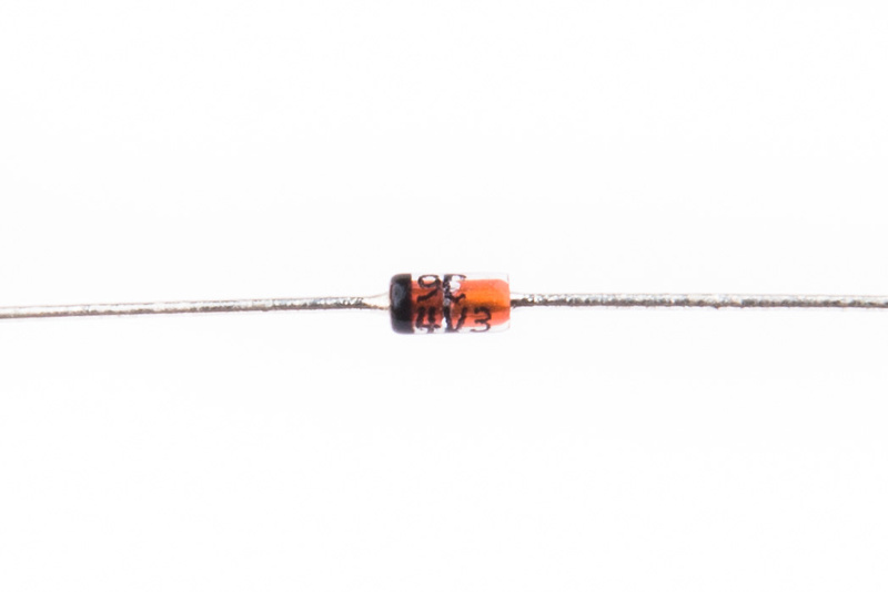
And CR10 looks like this:

p852784507-4.jpg


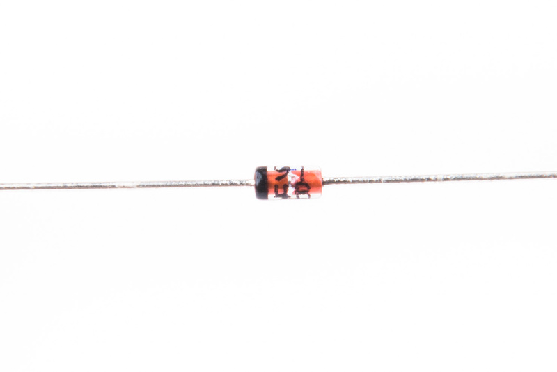
CR1-CR5, CR8, CR11, and CR12 look like this:

p971362080-4.jpg


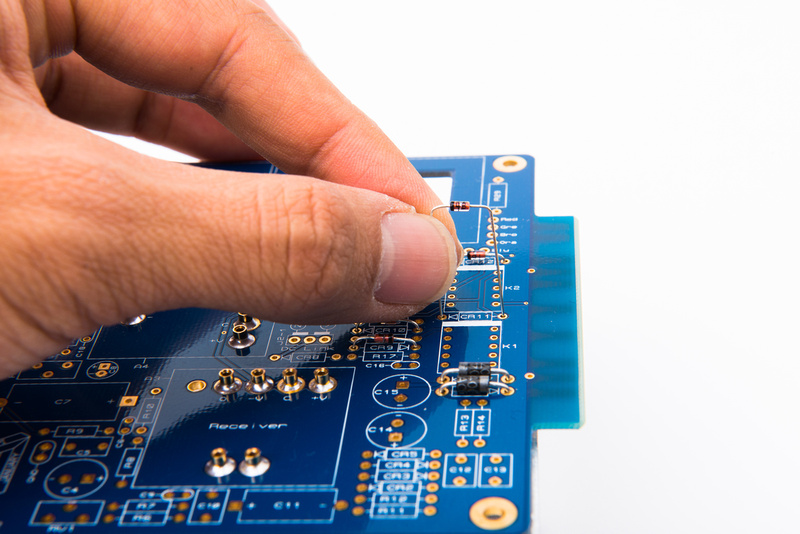
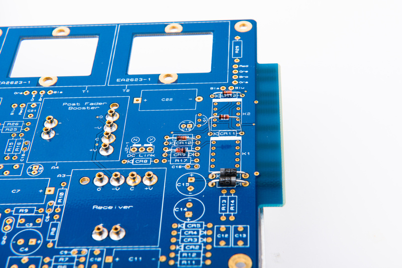
Next, populate the diodes making sure to set the side with the perpendicular line on the component facing towards the silk screened triangle on the PCB.

p586778555-4.jpg


Take the time to confirm proper orientation of all the diodes.

p604969520-4.jpg


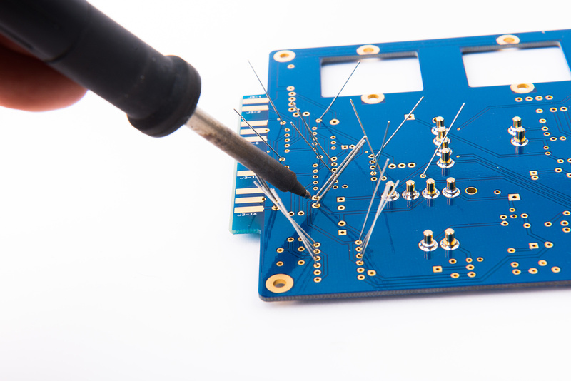
Bend the leads sharply near the PCB to hold the diodes in place and then solder each connection.  The aim is to keep the iron on the piece as short as possible while flowing a nice bead of solder that transfers a to the opposite side of the board, so both sides have a smooth fillet.

p628689862-4.jpg


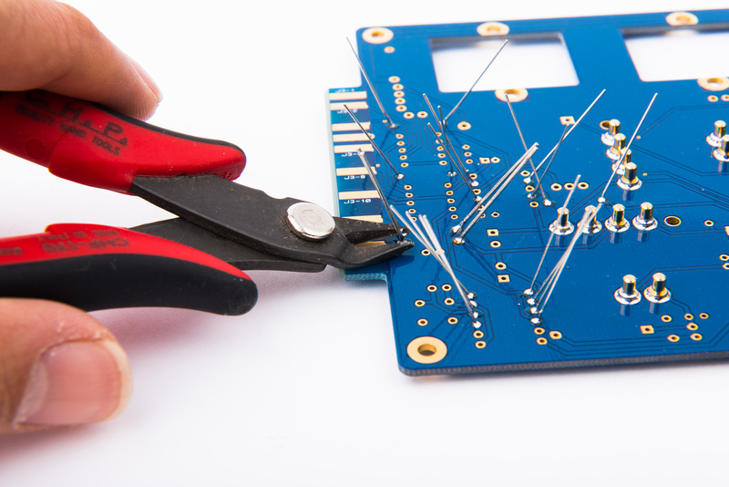
After soldering, trim the excess leads close to the PCB.

p773065756-4.jpg


p866616271-4.jpg


And, it never hurts to clean the board a bit while we have full access.

p862185019-4.jpg


Next, populate the resistors in similar fashion.  It does not hurt to verify resistor values with a multimeter before bending and inserting them into the board.

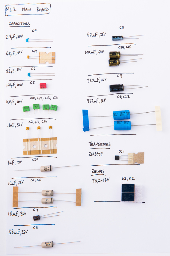
Next, locate and identify the capacitors and relays for the main PCB.

p788830977-5.jpg


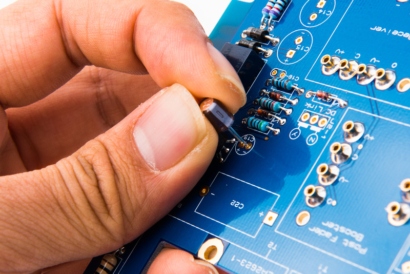
Pay attention to the polarity of the electrolytic capacitors.  The side with the line corresponds to the "-" marking on the PCB.  The end with the longer lead should go into the side marked "+".

p933458142-4.jpg


Some of the axial capacitors also have polarity so watch for the perpendicular line indicating "-" side.  We want to avoid smoke and excitement when we power up!

p777479226-4.jpg


Here, the capacitors are populated.

p667508151-4.jpg


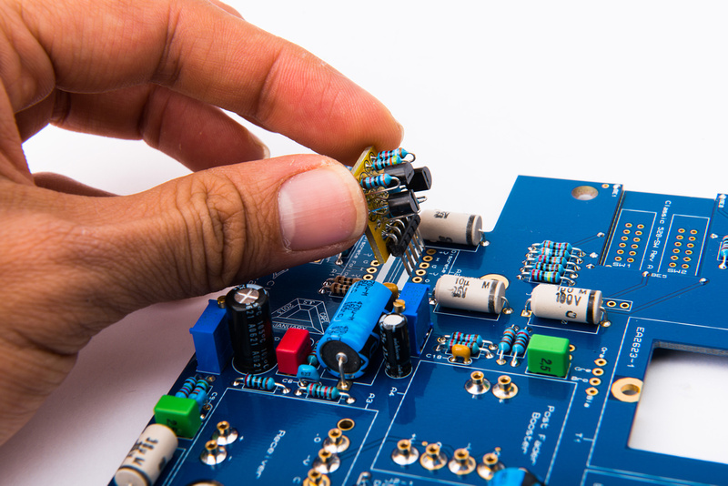
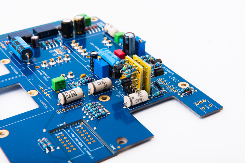
Next, install the previously built discrete follower boards onto the main PCB.

p641021523-4.jpg


p655901077-4.jpg


I have made a few slight alterations to the final steps of the ML2 Assembly Aid. The latest version has been uploaded for your viewing pleasure.
 
Is there a CMRR adjustment guide for the VC528 ML?  I've been reading over the CMRR guide for the VC528 ST2 but there seem to be difference.
 
The overall concept is identical to the first version. Most people have been buying my Extension Jig which has the proper R's fitted to it as well as instructions. There is a pic in the ML2 Assembly Guide that shows where to measure the signal.
 
Well, I had a good time building the gar2520 DOAs and the VC528 ML2 but now I'm stumped.

After finishing the build I ran the CMRR calibration with the CAPI extension jig.  Everything seemed to go fine but now that I'm running audio through it I find there to be a serious lack of low frequencies.  The frequency response starts to roll off around 4K and at 100Hz the unit shows -13db from flat.  There is also a less pronounced high frequency roll off.  I swapped A3 with A4 (DOAs) and while this had just the tiniest affect on the frequency response of the unit it did create a 3.7db drop in the output.  You can view a frequency response chart below. I generated this by sending a 20Hz to 20K sine wave sweep through the unit both before and after swapping A3 with A4.

I built the DOAs from the kit available from classicapi.com.  I'm hoping someone here can help me out. Does the information above give any hints that my problems might be with the DOAs?  Does the -3.7db output drop give an indication of which DOA might be the problem?  I don't have any other units to swap these into for testing so I'm wondering if I should buy another DOA kit or spring for one of the fully built & tested 2520's.

Any suggestions would be greatly appreciated.

Thanks.

p.s. One other detail about the testing of my VC528: The wacky frequency response curve is unaffected by the bypass switch. If I toggle it into bypass the lows freqs still roll off but the overall output of the unit jumps up by 8db.

VC528_freq_response-20140202-134847.png

 
Well it seems like there may be a few issues coming into play. The bypass switch is a hard bypass so the relays directly connect the input pins to the output pins. So if that part of the circuit is working properly, the odd freq response is not module related but coming from the rack, cable, interface etc. You can check continuity while using the extender card. When bypassed, card edge pin 2 should connect to pin 10 and pin 4 should connect to pin 8. You should also be able to hear both relays clicking when flipping the bypass/active toggle.

The fact that there is a level change when swapping opamps, definitely suggests one or possibly both of the opamps have issues.

It is very hard, typically impossible to troubleshoot a fresh module build with 2 fresh opamp builds. You need something known and good to test the opamps in or known to be working opamps to test in the ML2. I would suggest a couple of prebuilt opamps of some sort like maybe a pair of red dots from Scott.
 
Yeah.... too many variables.  I get it.  I just emailed Scott Liebers about purchasing a couple of his opamps.  Thanks for the tip on checking the bypass switch.  I'll poke at that and report back when I get the red dots. 

Thanks again.
 
jsteiger said:
Well it seems like there may be a few issues coming into play. The bypass switch is a hard bypass so the relays directly connect the input pins to the output pins. So if that part of the circuit is working properly, the odd freq response is not module related but coming from the rack, cable, interface etc.

I ran a sweep through my converter, through the rack with a different module (bypassed) and back and I got a very flat response.  There was a bit of a roll off in the very low freqs but nothing like what I get with the VC528.


jsteiger said:
You can check continuity while using the extender card. When bypassed, card edge pin 2 should connect to pin 10 and pin 4 should connect to pin 8. You should also be able to hear both relays clicking when flipping the bypass/active toggle.

Well... I seem to have a problem with my bypass circuit.  I get continuity between 2&10 as well as 4&8 all the time.  Regardless of the switch position.  When I flip the switch to ACT I can hear at least one of the relays click but when when I flip the switch up into the BYPASS position all I hear is the switch, I hear no relay clicking.

I checked the solder points on the switch and the relays.  I double checked the polarity of the relays as well as the diodes around the general area. I looked up the datasheet on the switch and checked it's terminals in both positions and it's functioning correctly.  There's something obvious that I'm missing.
:-\
 
Can you post a pic of that section of the board? The most common error is not identifying the 4V3 zener diode. The bypass switch is either connecting ground to the relay control circuit or leaving it open.
 
Well, nothing is jumping out at me but I also cannot tell the parts numbers on CR9 and CR10.

Do the Bypass status LED's work as expected?
 
Yes, the bypass LEDs work correctly.  With a magnifying glass I can make out "4v3" on CR10 and I think "24" on CR9.

 
Back
Top