Class A stuff from EW+WW

GroupDIY Audio Forum

Help Support GroupDIY Audio Forum:

This site may earn a commission from merchant affiliate links, including eBay, Amazon, and others.

clintrubber

Well-known member
Joined
Jun 3, 2004
Messages
6,015
Location
The Netherlands
Came across a few circuits that might come in handy.

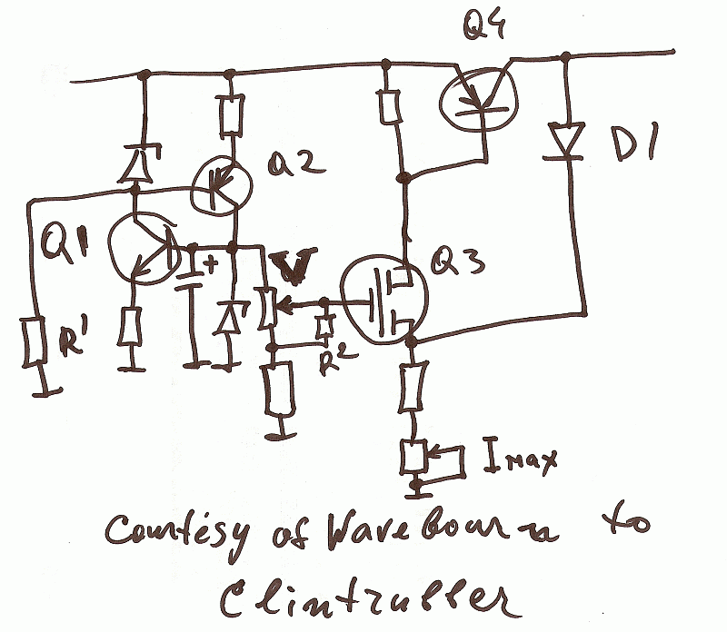
FWIW, here we have an adaptive biasing class A circuit and
an accompanying supply filter (using the output impedance
of a current mirror to extremify the ripple-reduction).

Thanks Mr. Macaulay & EW+WW :thumb:


BTW, would RN have considered adaptive class A before he went
away from BA283 to tackle the heat buildup ?


small version:

clA_small.jpg


download (383kb):

http://www.twin-x.com/groupdiy/albums/userpics/clA.jpg


Enjoy,

Peter
 
Thanks for the scan.

I doubt that this biasing scheme provides the low distortion of true class A. It seems to avoid charge storage effects but not crossover-distortion.

The PSU circuit is cool but I'm not sure if it qualifies as a "capacitor multiplier" as it rather seems to be a buffered voltage reference/emitter follower. Replacing PR1 with a zener would make the circuit more effective IMO.

Samuel
 
[quote author="Samuel Groner"]Thanks for the scan.[/quote]

My pleasure.

You didn't fail, I knew beforehand there were some critical points from you upcoming. :wink:

Note I didn't build this (yet), just found it when sorting out some papers.
Also added FWIW for that reason, not sure about the real or effective merits of these circuits.


OK, let's see

[quote author="Samuel Groner"]I doubt that this biasing scheme provides the low distortion of true class A. It seems to avoid charge storage effects but not crossover-distortion.[/quote]
Very well possible! But what makes you think so ?

The PSU circuit is cool but I'm not sure if it qualifies as a "capacitor multiplier" as it rather seems to be a buffered voltage reference/emitter follower.
In general, multiple valid names for a certain topology may exist I'd say.
Some will be better or more correct than others, but I wouldn't say the "capacitor multiplier" label is invalid here. Makes it insightful what's happening here.
Better ways may exist, but don't make another one invalid.

Replacing PR1 with a zener would make the circuit more effective IMO.
I'm with you on that.
And making it an active zener (by adding just one more BJT, in // to PR1, base to wiper - or use an additional R between b & e and connect PR1 between b & c) would keep the adjustability.

Best regards,

Peter
 
[quote author="Samuel Groner"]I doubt that this biasing scheme provides the low distortion of true class A. It seems to avoid charge storage effects but not crossover-distortion.
Very well possible! But what makes you think so?[/quote]
It is my understanding (which might be wrong) that the low distortion in class A is mainly a result of having constant transconductance (i.e. constant emitter current) in the active transistor for any given voltage below clipping. The circuit shown does not provide this property.

Some will be better or more correct than others, but I wouldn't say the "capacitor multiplier" label is invalid here. Makes it insightful what's happening here.
IMO it is very misleading--it shows what's not happening here. A "true" capacitor multiplier has the potential of multiplying a given real capacity by the hFE of the series transistor. The circuit shown does not multiply any capacity--in fact you could skip C1 without loosing too much ripple rejection (with the actual performance now depending mostly on the CCS PSRR). If it were a capacity multiplier it would need to loose its ripple rejection as zero times a large number is still zero.

In addition to this, a capacity multiplier has no regulation at DC as the impedance of the capacitor is infinite there. The schematic shown has DC regulation (though pretty poor--get the zener ready).

Samuel
 
[quote author="Samuel Groner"]
Some will be better or more correct than others, but I wouldn't say the "capacitor multiplier" label is invalid here. Makes it insightful what's happening here.
IMO it is very misleading--it shows what's not happening here. A "true" capacitor multiplier has the potential of multiplying a given real capacity by the hFE of the series transistor.

Samuel[/quote]

Hi Samuel,

So far I didn't think further than: if this ( http://en.wikipedia.org/wiki/Capacitance_multiplier) is a capacitance multiplier (as at least is commonly used for this kind of circuit, needn't be true because of just that, but still...) then a version with an R-realisation by means of a current mirror is still a capacitance-multiplier I'd say.

The circuit shown does not multiply any capacity--in fact you could skip C1 without loosing too much regulation. If it were a capacity multiplier it would need to loose its regulation as zero times a large number is still zero.

Maybe we should think the mentioned zener still not present and talk about filtering, not regulation, so I'm not sure how this would change your sentence above.
This following is a bit lame, but in principle there's always some node-capacitance which gets treated by the hFE_3 * hFE_4. In combination with the large R from the CM you'd still get usuable filtering I expect, but nothing beats actually trying.

Best regards,

Peter
 
Maybe we should think the mentioned zener still not present and talk about filtering, not regulation, so I'm not sure how this would change your sentence above.
You may need to re-read my previous post--I edited it before you posted.

In any case the circuit discussed has regulation and ripple rejection without C1 (or any parasitics) being present, with or without zener.

Samuel
 
A first, for lower voltages (below 50V input) R2 has to be increased proportionally. Second, output voltage will depend very much on Vbe of the upper left transistor and vary with temperature. Third, it will be destroyed easilly when shorted out occasionally since if a Darlington pair has say total beta of 5000 output current when shorted will be about 5A. Fourth, output voltage will depend very much on a load (base current of Darlington pair decreases voltage drop on a variable resistor). And fifth, despite of a good reference voltage source ripples will depend on a Darlington's total beta as well.

Use at least 10 times more current from a CCS and a Zener instead of a pot, though anyway output transistor is not protected, but at least output voltage will be more stable.

I can draw you a PS with the same number of transistors that will be free from all mentioned above drawbacks.

Speaking of the amp, it is not a class A amplifier, though it tries to keep transistors always conducting using a feedback with frequency dependent phase shifts on highs. I'm afraid it will oscillate well requiring some tweaking of poles.
It reminds me a story about 8 helpers to screw a bulb into a socket in a ceiling.

[quote author="Samuel Groner"]
It is my understanding (which might be wrong) that the low distortion in class A is mainly a result of having constant transconductance (i.e. constant emitter current) in the active transistor for any given voltage below clipping. The circuit shown does not provide this property.
[/quote]

You could be right if we were so happy to have a triode and anti-triode, a transistor and an anti-transistor... My amp that keeps output transistor on always the same current contains a special voltage to current converter while a classical class A amps are loaded on constant current (single ended) or have pair of identical output devices. In first case while current supplied by CCS or a choke/transformer is nearly constant, a load consumes current.

Anyway, people are using their brain instead of copying other's designs, that is very good indeed!
 
[quote author="tv"]I don't trust the R12 (39K) on the amp schem.[/quote]

Yeah, I've missed that! :cool:

Consider it as a typo. Probably the author had 2 schematics: for unipolar and bipolar power supplies, so drawing it for the article he made a typo. :grin:
 
Consider it as a typo.
I consider it a smoke maker. Cool concept nevertheless. I like small aclass amps, they make small speakers sound bigger then they are and smoother while not that much more expensive compared to ab designs. I would mod the schemo with cheap mc33178 that's aclass already. Hoopefully it would be able to drive the output transistors.
 
I think you should look at these shecmatics as hints, not as being complete. the adaptive biasing thing is something Ive been toying with for a while myself. the way I see it the control loop should be sort of like a compressor sidechain, very fast attack, very slow release. ie, the first time the amp needs more current (and clips) it instantly gets the bias bumped up. it wont clip next time. ideally the standing current should overshoot the instantaneous requirement by a small amount and then freeze. could use cap+FET sample and hold circuit, but IMO this is asking to by done digitally.

mike p
 
[quote author="mikep"]I think you should look at these shecmatics as hints, not as being complete.[/quote]
Indeed, note these posted scans are from EW+WW 'Circuit Ideas',
might have added that. In other words, they're not
necessarily production-ready blameless designs that can withstand
all kinds of abuse.... yet ! Hence: ideas.

Nevertheless I can't imagine the circuit will self-destruct, the author will most likely have made at least a breadboarded version before submitting.

That R12 is fun indeed, most likely because of as pointed out. Note though that EW+WW aren't blameless w.r.t. their schematic-drawings: over the years various very obvious mistakes have appeared, giving the impression the person doing the conversion from back-of-envelope to artwork isn't experienced in the electronic field (unsurprisingly/understandable for such a job).

Regards,

Peter
 
[quote author="Wavebourn"]I can draw you a PS with the same number of transistors that will be free from all mentioned above drawbacks.[/quote]
Let's have it ! :wink:

Regards,

Peter
 
[quote author="Wavebourn"]They should call it "Stupid Ideas". :green:[/quote]
Do you think this one is worse than the Schoeps circuit ? :green: :wink:

Honestly, I more than appreciate the various reactions. Note that I just ran across it and thought it'd at least be worth to scan & put it up for discussion, but note I didn't build it or necessarily considered it to be a mighty perfect circuit...
But OK, on to my point here: it also made me wonder if it'd be possible to have a thread with posted circuits that everybody 'agrees' on... (FWIW, but just curious)
So no further improvements possible (without going overboard w.r.t. component count, dissipation, voltage rails, board space, esoteric parts etc), in three words: blameless, perfect, elegant. And to keep it 'unbiased': preferrably from someone else than the submitter. Any circuits that come to mind ?

Regards,

Peter
 
[quote author="clintrubber"][quote author="Wavebourn"]I can draw you a PS with the same number of transistors that will be free from all mentioned above drawbacks.[/quote]
Let's have it ! :wink:

[/quote]

Hereyougo:

peteps.gif


R1 is needed when Q1 and Q2 are too clean (low c-b current) so a reference voltage source (very nice one!!!) won't start. Some voltage divider and a diode to supply an initial voltage would be better theoretically, but not too much practically. Instead of an upper Zener a LED may be used as a pilot light.

If you want a better thermal stability you may replace D1 by one more FET turning back to a true diff-cascade, or use a LED to indicate voltage stabilization.

Not good for production "as is", but enough of DIY ideas, right?
 
[quote author="clintrubber"]
But OK, on to my point here: it also made me wonder if it'd be possible to have a thread with posted circuits that everybody 'agrees' on... (FWIW, but just curious)
So no further improvements possible (without going overboard w.r.t. component count, dissipation, voltage rails, board space, esoteric parts etc), in three words: blameless, perfect, elegant. And to keep it 'unbiased': preferrably from someone else than the submitter. Any circuits that come to mind ?
[/quote]

Here you go: class A output stage. Single point input, overload protection, symmetrical and linear, wide bandwidth (I used b-c junctions instead of diodes).

beag-hybrid.gif


Actually it is made of 2 complementary opamps loaded on each other, connected as voltage followers. Diodes instead of transistors are used because b-e breakdown voltage is usually very low (I saw only one transistor that had nearly equal b-c and b-e breakdown voltages, but it was a small signal one).

Can you improve it (except current mirrors instead of resistors between b-e of output transistors)?
 
[quote author="Wavebourn"]They should call it "Stupid Ideas". :green:[/quote]
Sorting out that pile of schematics I also ran into a 555-timer circuit with a negative resistance to trigger stuff before the start-button was pressed :cool:

Thanks for the posted schematic, will have a further look later today :thumb:
 
[quote author="clintrubber"][quote author="Wavebourn"]They should call it "Stupid Ideas". :green:[/quote]
Sorting out that pile of schematics I also ran into a 555-timer circuit with a negative resistance to trigger stuff before the start-button was pressed :cool:

Thanks for the posted schematic, will have a further look later today :thumb:[/quote]

You are welcome!

Can you improve them? :green:
 
Back
Top