Andy Peters
Well-known member
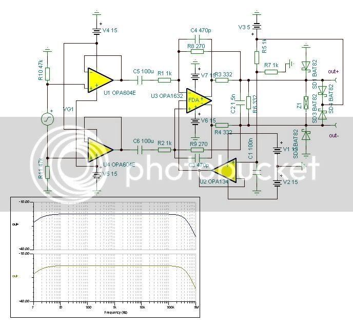
Moby said:I'm asking myself the same thing, but must be because of filter at the end of first stage. It looks like some kind of pre-emphasis filter or something....I wonder is it possible to avoid this filter and also to add some more current capable amp to drive 332+332ohnm terminated input of AD5393 :?:
The 332-ohm resistors aren't "terminations" that require any significant current source. Look again at the schematic -- those resistors are in series with the driving op-amp, not a load to ground!
These resistors help isolate the driving op-amp from the capacitive load presented by the ADC and the input load cap (the cap across the ADC inputs). Reducing them could be bad if the op-amp can't handle the load. Increasing them beyond some value will increase setting time.
So the resistors aren't the problem -- the capacitance is.
-a