


Matador
Well-known member
This is a feeler for an experimental/prototype PCB meant to be installed as a replacement for the many popular Chinese U87 clone bodies (from companies like Aurycle, MXL, Nady, Carvin, etc). Most of these bodies can hold two of these boards.
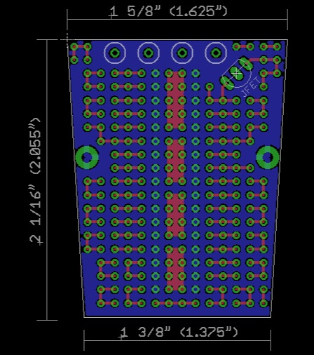
The board features a prototype grid much like what would be found on commercially available Veroboard systems. The boards feature an interconnected grid of 0.1" spaced plated through holes, which are grouped into nets of 3 or 4 holes. Net's can be bridged through components like resistors or capacitors, or can be wired from net to net under the board vertically with small 22-26 gauge wire to make net groups the same.
Basic features:
1) 4 teflon standoff's along the top for Hi-Z connections to capsule backplates or diaphragms (most mikes typically use at most 3, however if one wanted to experiment with providing different bias points for individual backplates this would be possible)
2) One JFET component footprint for the main input amplifier, with the gate pin pointed at the rightmost Hi-Z connection point
3) 44 net groups of three or four holes
4) 36 ground nets
5) 4 VDD groups, each with 8 to 10 connections, connected through copper pours on the top copper. This provides for up to 4 cascaded pi-filters for VDD with at minimum fanout of 7 to other traces
6) Full copper pour of ground node on the bottom
7) 7 net groups along the bottom for connecting to transformers and XLR sockets.
I can also add to the top silk layer with all of the top layer interconnections in case the traces are difficult to read through the solder mask.
I am thinking standard FR4 boards, 0.063" thickness with 1 oz copper.
For price, and depending on the interest, I'm looking at a cost of $20 per board set, which would include:
1) 4 Keystone Teflon standoffs
2) Two of the above boards
3) Shipping anywhere in the US via USPS in a flat rate padded envelope
Please post a reply here if you are interested, along with the quantity.
I may also add a keepout of the ground pour on the bottom under the Hi-Z connections. With my design rules, the soldermask should completely cover the ground pour and the annular rings should be well isolated, but when dealing with 1G impedances better safe than sorry.")
Also, since I haven't contacted my fab house, any reasonable changes/suggestions are welcome.
The board features a prototype grid much like what would be found on commercially available Veroboard systems. The boards feature an interconnected grid of 0.1" spaced plated through holes, which are grouped into nets of 3 or 4 holes. Net's can be bridged through components like resistors or capacitors, or can be wired from net to net under the board vertically with small 22-26 gauge wire to make net groups the same.
Basic features:
1) 4 teflon standoff's along the top for Hi-Z connections to capsule backplates or diaphragms (most mikes typically use at most 3, however if one wanted to experiment with providing different bias points for individual backplates this would be possible)
2) One JFET component footprint for the main input amplifier, with the gate pin pointed at the rightmost Hi-Z connection point
3) 44 net groups of three or four holes
4) 36 ground nets
5) 4 VDD groups, each with 8 to 10 connections, connected through copper pours on the top copper. This provides for up to 4 cascaded pi-filters for VDD with at minimum fanout of 7 to other traces
6) Full copper pour of ground node on the bottom
7) 7 net groups along the bottom for connecting to transformers and XLR sockets.
I can also add to the top silk layer with all of the top layer interconnections in case the traces are difficult to read through the solder mask.
I am thinking standard FR4 boards, 0.063" thickness with 1 oz copper.
For price, and depending on the interest, I'm looking at a cost of $20 per board set, which would include:
1) 4 Keystone Teflon standoffs
2) Two of the above boards
3) Shipping anywhere in the US via USPS in a flat rate padded envelope
Please post a reply here if you are interested, along with the quantity.
I may also add a keepout of the ground pour on the bottom under the Hi-Z connections. With my design rules, the soldermask should completely cover the ground pour and the annular rings should be well isolated, but when dealing with 1G impedances better safe than sorry.
Also, since I haven't contacted my fab house, any reasonable changes/suggestions are welcome.
